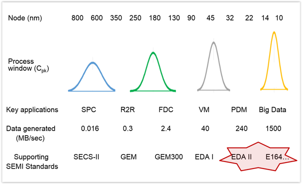
Anticipating and promoting the increased adoption of SEMI’s Equipment Data Acquisition (EDA / aka Interface A) standards, we’ve posted a number of blogs over the past 12 months to address questions that potential stakeholders have repeatedly asked across the value chain. These postings have dealt with everything from the factory applications enabled by EDA to the best practices for OEM implementation of these standards to the development of robust equipment purchasing specifications.
Since the adoption process has now clearly reached critical mass, we must seriously address the question “How are we going to test the equipment and systems that incorporate these standards?” in a way that supports the entire industry. It’s an excellent question, and one that has a multi-part answer.
![]()
Given the structure and expected use of the EDA standards, the acceptance testing process for a unit of semiconductor manufacturing equipment will include at least three components, each of which addresses a different aspect of the standards. Note that we’re explaining this from the perspective of the end customer in a semiconductor factory, since this is the most common use case, but most of the same principles apply when testing EDA client infrastructure/application components as well.
-
Compliance testing – does the equipment adhere to the specifications described in the SEMI Standards, and were these specifications interpreted correctly? Will it cleanly connect to the EDA client infrastructure without modification or extensive configuration?
-
Performance and stability testing – does the equipment meet the end users’ performance and availability specifications in terms of data sampling intervals, overall data volume transmitted, size and number of DCPs (data collection plans) supported, demands on the computing/network resources, up-time, etc.? Will it support the range of application clients expected in a production environment?
-
Equipment metadata model conformance testing – does the equipment model delivered with the interface represent the tool structure and content anticipated by the end customer? If the customer has requested that SEMI E164 (EDA Common Metadata) be fully supported, does the metadata model meet these specifications?
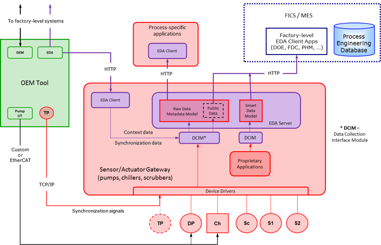
Of course, in addition to the requirements dictated by the standards themselves, most advanced semiconductor manufacturers will have a number of factory-specific requirements that must also be supported by the EDA interface. These may include special events and data for particular automation schemes, vectors of process parameters to support fault detection applications or other feature extraction algorithms, synchronization signals for external sensor integration, and the like. To address these requirements efficiently, an EDA test system should be extensible by its users.
You can see how interesting and vital this topic becomes when you consider the range of requirements outlined above. We’ll explore each of these in more detail in the next few postings, so stay tuned!


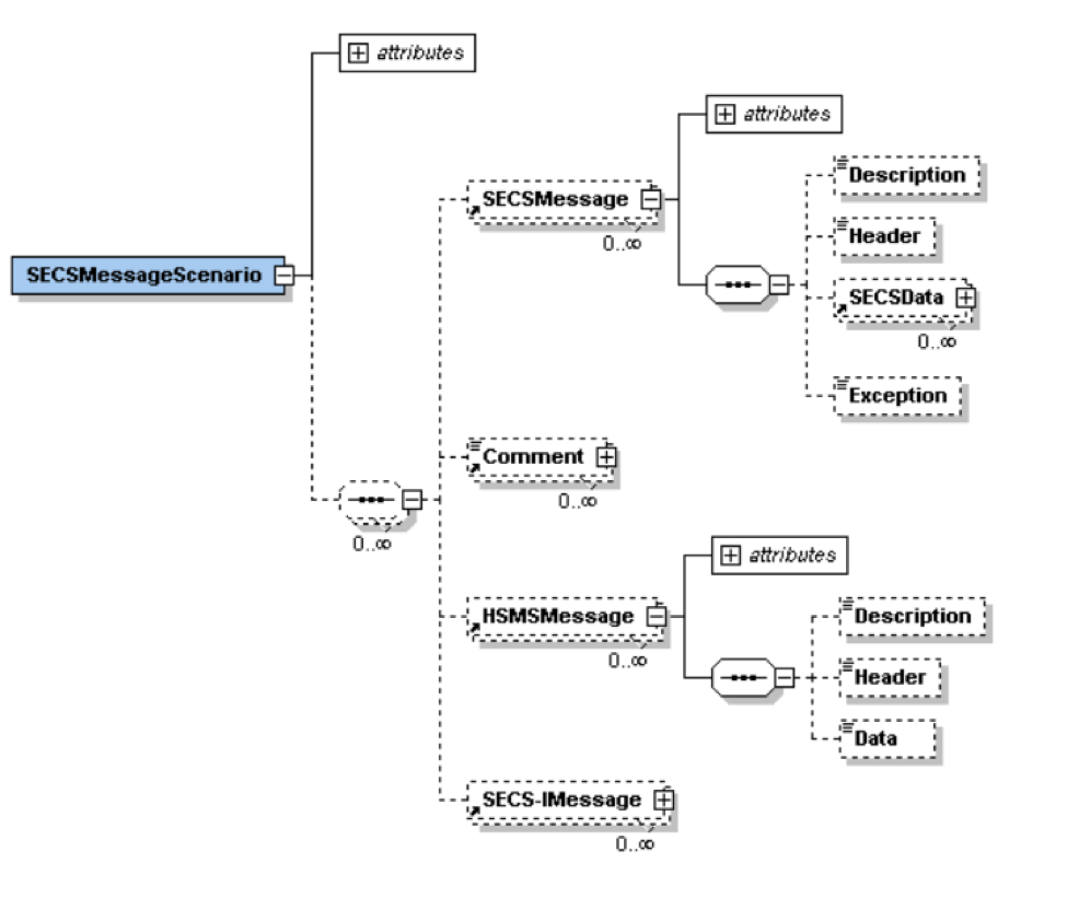
 In a previous blog we mentioned that two new SEMI standards, E172 and E173, demonstrated that the GEM standard was alive and well and even gaining new momentum by evolving to adopt new technology. The earlier blog focused on E172 with its SEDD files that use an XML schema to describe what is in a GEM interface. Today’s blog is about the E173 Specification for XML SECS-II Message Notation: a new way to log and document GEM/SECS messages, again using an XML schema.
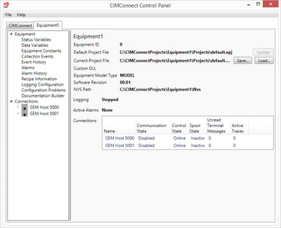
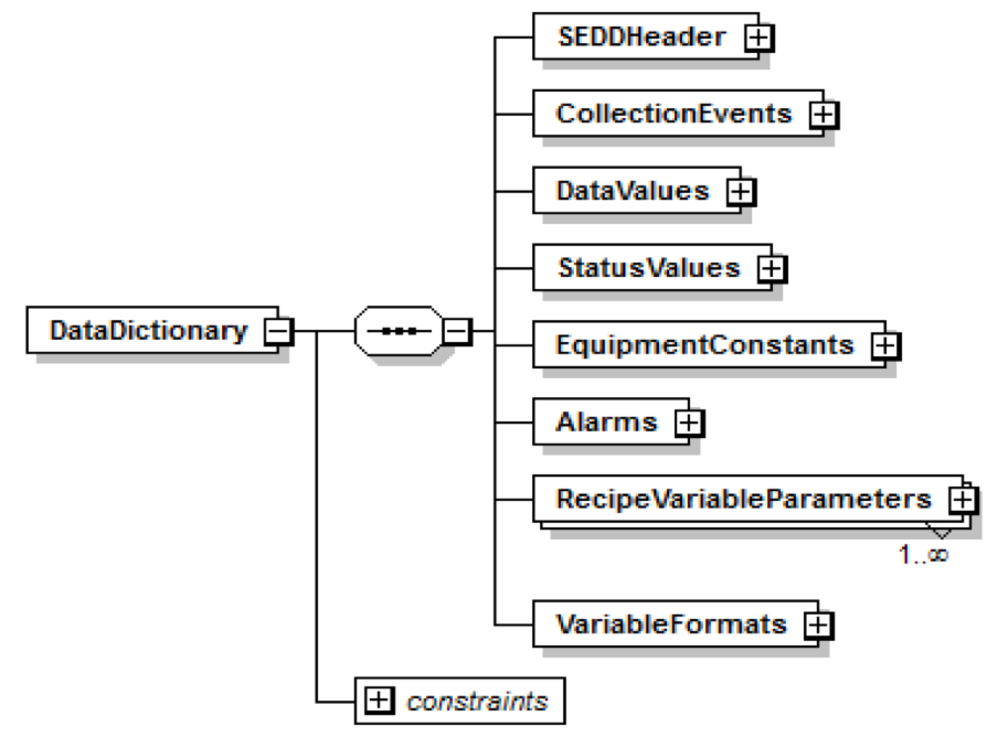 So essentially the SEDD file includes a list of the data available for collection by a host, some general information about the equipment (in the header), and the format of the data variables, status variables and equipment constants. As an example of what details are included, here are the details for collection events.




 Cimetrix and our new distribution partner, Linkgenesis, participated in a joint booth at SEMICON Korea last week in Seoul. With over four exhibit halls located in the COEX Convention and Exhibition Center, SEMICON Korea is the largest SEMICON in terms of number of visitors—about 40,000—and included over 1,870 booths in 36,000 sq. meters of show space. The theme of the show was “Connect to Future, Market, People and Technology” with keynote speakers from leaders at Synopsys, Texas Instruments, and Audi. The show was co-located with LED Korea. Included in the schedule was also a meeting for the Information and Control Technical Committee, Korea Chapter, to work on SEMI standards.
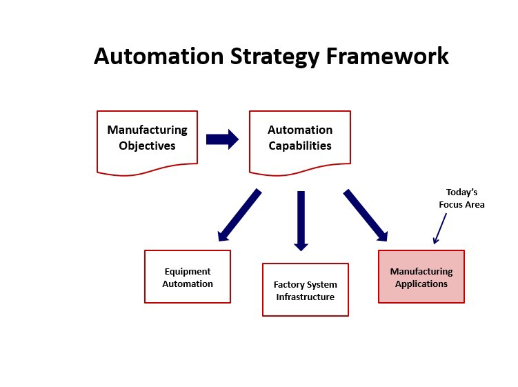
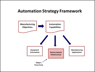 However, before diving into a detailed design process for an EDA factory system, you must decide what overall system architecture will govern that design. A number of factors go into this decision, including 1) the functional requirements that distinguish EDA-based data collection from other more traditional approaches, 2) technology constraints of the existing factory systems, 3) budget limitations, 4) schedule requirements, and especially 5) the non-functional requirements (scalability, performance, reliability, ease-of-use, etc.) that often make the difference between success and failure of a given system.
