xby David Francis
Product Manager, Connectivity Products
Back in the 1990s, Joe Diffie released an album titled “Third Rock from the Sun.” I have to admit I liked the title song, especially the chorus:
“Cause and effect, chain of events
All of the chaos makes perfect sense
When you're spinning round
Things come undone
Welcome to Earth 3rd rock from the Sun.”

At the time, I was working with Motorola in Austin developing host-side cell control applications for one of their new fabs. Motorola had implemented some rudimentary equipment control and data collection in their older fabs, but the standards were loosely defined at that time and the equipment interfaces were inconsistent. We realized we could not replicate the work implemented in the old fabs into the new fabs, yet we did not have solid standards to use for the new fabs. As the song said, we were “spinning round” in this chaos.
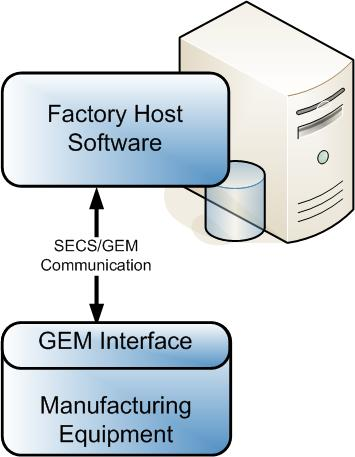
What eventually drove more clarification in the GEM/GEM300 standards was the industry-wide push to move to fully automated 300mm IC manufacturing. The larger wafers offer much greater productivity and throughput, with significantly lower cost per die, and SEMI wanted to ensure the industry had a well-understood and approved interface standard for the equipment used to manufacture semiconductors on these much larger wafers. Those new standards made it easier and more cost effective to create the host-side cell control applications. Now the chaos started to “make perfect sense.”
Embracing the GEM/GEM300 standards allowed IC manufacturers to purchase standard software components to analyze manufacturing processes and identify opportunities to increase productivity. In other words, they wanted to bring order to all the chaos. The alternative – developing their own data analysis applications for each fab – would have been very expensive and time consuming. SEMI brought order to the scene by offering the GEM/GEM300 standards that all the equipment vendors and fabs could use. Now OEMs could develop equipment needed for automated wafer processing with the confidence fabs could install the machines and link them to their networks. Fabs could increase throughput and drive down cost per die, and, just as important, gather data necessary to increase manufacturing efficiencies even more.
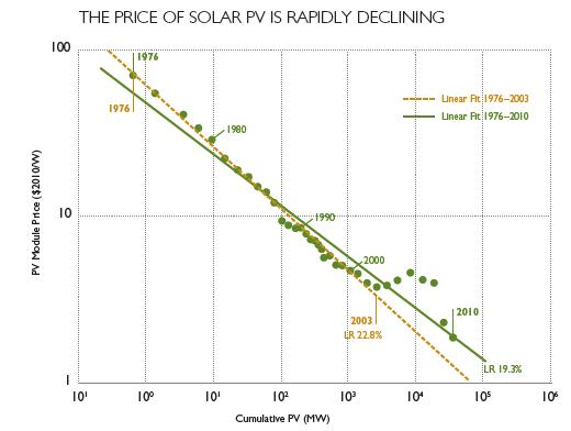
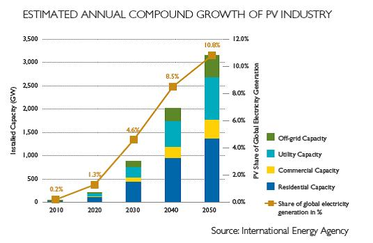
Fast forward twenty years, and we see a very similar situation, this time caused by the impressive growth in Photovoltaic cell and LED manufacturing. The fabs in those industries need more advanced equipment to increase throughput and drive down unit costs in order to meet demand. However, up to this date, both sectors are reluctant to adopt the GEM standards. They are concerned those standards may be too big and complex for their processes, which are simpler than the current state-of-the-art semiconductor fab processes. Once again, we see the chaos that occurs with explosive growth and companies seeking a solution to bring order to their processes.
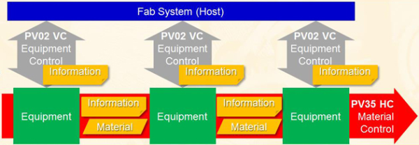
Since I’ve seen this story before - and heard the music played time and time again - I know that adopting communication standards will help PV and LED manufacturers continue their drive to reduce unit costs and drive demand. The effort is underway in the PV sector with the PV2 standard. The LED sector should also look to adopt existing standards, or do what the PV sector has done and develop their own standards. Either way, we know that standards help all the “chaos make perfect sense.”
 The Cimetrix Resource Center is a great way to familiarize yourself with standards within the industry as well as find out about new and exciting technologies.





 and public speaker has been speaking and writing about the imperative need for American transition toward green energy for some time. His profound belief in superior American ingenuity and innovation, coupled with the rapidly growing world appetite for energy, is the potent recipe which should be directing our creative and practical energies toward a shift in US mentality that is not only good for our collective health, but also spells opportunity.
