Background
The North America Information & Control Committee (I&CC or NA I&CC) is comprised of several task forces including GEM 300, Diagnostic Data Acquisition (DDA), Advanced Backend Factory Integration (ABFI), Fab & Equipment Computer and Device Security (CDS), and Graphical User Interfaces (GUI). These task forces and the committee all met during the week of SEMICON West, July 11-13, 202. Not long ago, SEMI regulations were modified to allow TC Chapter (Committee) voting in virtual meetings; therefore, the standards activities continue to move forward. In-person task force participation was much higher than the last meetings, but remote participation also remains strong. This blog is a summary of the activities in each task force.
GEM 300 Task Force
Here is a summary of worldwide activities related to the GEM 300 task force as of the start of the GEM 300 task force meeting.
|
Region |
Ballot |
Standard(s) |
Status |
Topic |
|
Korea |
5832 |
New |
? |
Generic Counter |
|
NA |
6572 |
E30 |
Adjudication |
Add Stream 21, more stream 2, Cleanup Process Program Management. |
|
NA |
6835 |
E87 |
Development |
Carrier Ready to Unload Prediction update |
|
NA |
6836 |
E87/E90 |
Development |
Extending substrate characteristics, such as for Bonder/Debonder support and other applications |
|
NA |
6859 |
E116 |
Adjudication |
Recommendations from the ABFI task force |
|
NA |
6893 |
E5 |
Published |
Errata |
|
China |
6914 |
E87 |
Development |
Modify E87 to allow for more equipment adoption, particularly in the semiconductor backend. |
|
NA |
6916 |
E5 |
Adjudication |
FormatCode for OperatorCommand. Various Errata. |
Three ballots were adjudicated during the GEM 300 task force meeting. The term “adjudication” means we review the voting and recommend handling of all negative votes and comments received to ultimately accept the ballot for publication or reject the ballot for rework. The recommendations by the task force are then finalized at the committee meeting. Usually, the task force recommendation is accepted by the committee, as was the case in all three ballots.
6916 E5
This ballot proposes to modify the E5 SECS-II standard and included the following minor changes:
- Allow data variable OperatorCommand to be type ASCII.
- Correct various typographical errors
- Remove the dependency between variables MDLN (equipment model number) and EqpSerialNum (equipment serial number).
This ballot passed after the only negative was withdrawn by the voter.
6572B E30
This ballot proposes to modify the GEM (E30) standard. It is a revision ballot, meaning the entire E30 standard is subject to review. This is the third time the ballot has been submitted. It is a major update to the GEM standard and includes the following changes:
- Process Program Management changes
- The terms “recipe” and “process program” are currently used nearly interchangeably. The proposal is to use the term “process program” exclusively.
- References to E42, large formatted and large process programs are moved out of the main standard and into the appendix.
- Stream 21 messages are introduced for process program management, including both the single and multiple message techniques. This provides a simplified way for GEM interfaces to upload and download large process programs.
- The entire process program management section is vastly reorganized to help implementers understand the available alternatives and the scenarios for each available alternative. New tables were introduced to compare and summarize implementation alternatives.
- Collection event ‘Process Program Error’ is specifically listed as required, rather than just as an implied requirement.
- A series of new SECS-II messages are introduced including S2F51-S2F64. These are new capabilities to make a GEM interface more transparent.
- S5F7/F8 is added to the alarm management capability for similar reasons.
- Two new GEM documentation features are added and made available through the GEM interface using Stream 21 messages including PDF documentation and SEDD (see SEMI E172) documentation. This should make it easier to distribute GEM documentation and ensure that the right documentation is referenced.
- Two new equipment identification features are added, one to identify the equipment supplier and one to uniquely identify each individual equipment. This should make it easier to identify and track specific equipment on the factory floor.
- Some changes related to terminology are included. SEMI regulations recently were updated with a list of restricted bias terminology which are not allowed in any SEMI standards and a list of terms to avoid when possible.
This ballot failed due to a disagreement regarding a proposed change to the GEM control state model collection on transition 10 related to the host off-line state. The task force remains evenly divided on this issue; therefore, this change will be withdrawn from the next revision of this ballot.
I am optimistic that the 6572C revision of this ballot will pass voting with little controversy. This ballot has already been distributed to the task force for final review. Little controversy remains unless some voter raises a new issue.
6859 E116
Originally ballot 6859 intended to add significant new features to the E116 standard. However, the aggressive changes have been abandoned. Instead, this ballot is focused on making one change to E116. Currently the E116 specification implements collection events in a manner inconsistent with E30, E40, E87, E90, E94, E109, and E157. This E116 ballot failed. After further discussion in the task force, consensus on the proposed changes seems possible in the next voting cycle. The updated ballot 6859A has already been submitted for review by the task force.
DDA Task Force
The DDA task force has been and continues to update the Equipment Data Acquisition (EDA a.k.a. Interface A) standards with the goal to approve an EDA Freeze 3 set of standards based on gRPC technology. To date the following ballots have been completed:
|
Standard (Ballot) |
Ballot Status |
|
E138 (6336) |
Published - 03/15/2019 |
|
E120 (6434) |
Published – 05/30/2019 |
|
E145 (6436) |
Published – 05/31/2019 |
|
E178 (6300) |
Published – 01/10/2020 |
|
E179 (6803) |
Published – 03/11/2022 |
|
E132 (6719A) |
Published – 04/29/2022 |
|
E132.2 (6346F) |
Published – 04/29/2022 |
|
E125 (6718A) |
Published – 04/22/2022 |
|
E134 (6720A) |
Approved - In Publication Queue |
|
E134.2 (6347A) |
Approved - In Publication Queue |
|
E179 (6837) |
Approved - In Publication Queue |
|
E125.2 (6345A) |
Approved - In Publication Queue |
|
E125 (6891) |
Approved - In Publication Queue |
|
E179 (6892) |
Approved - In Publication Queue |
|
E120.2 (6908) |
Approved - In Publication Queue |
During these meetings, three DDA task force ballots failed adjudication, 6927 (E125, E125.2), 6928 (E132, E132.2) and 6929 (E134, E134.2) due to procedural errors which violated SEMI regulations. This is primarily due to a long backlog of publications on previously approved specifications. Discussions were held in several meetings in an attempt to find ways to help SEMI get caught up on publications. The delay in publication is partly due to the several large ballots that were backlogged when COVID activity prevented the committee from completing adjudication in remote or hybrid meetings.
Test Session #1
The most important activity for the DDA task force was “vender test session #1” held on Thursday, July 14. An open invitation was made to all task force members to participate in an E132 test session. Anyone could submit a client and/or equipment server implemented with the current E132 and E179 specifications. Four companies came together and ran tests against each other’s software. Each participant will provide the task force with a list of issues in E132 and E179. This was a great opportunity to try the gRPC technology together and get a sense of what issues still need to be resolved before EDA Freeze 3 is complete.
DDA Freeze 3 Plans
The DDA Task force plans an update to E125, E132, and E134 including changes from the recently failed ballots as well as topics raised in the test session. Due to the expanded scope, new ballot numbers will be issued. Additionally plans to update E164 are also moving forward. The biggest challenge for E164 will be converting the XML files into JSON files. Either JSON5 or JSONC will likely be used since comments are mandatory in the E164 complementary files which show how to create GEM 300 capable EDA equipment models.
ABFI Task Force
The Advanced Backend Factory Integration task force is actively working on two ballots.
One ballot is a minor update to the E142, the substrate mapping specification which facilitates traceability and other application where substrate, tray, feeder, and other information can be shared between a factory and equipment. The minor update will add additional substrate types so E142 substrate maps can be used in more applications.
Additionally, the task force is working on ballots 6924 and 6925. The 6924 specifications will define the management of Consumable and Durables on manufacturing equipment. Features include allowing the host to accept or reject newly mounted consumables and durables. Additionally, the equipment will be able to report on consumable and durable usage. While technically both can already be done, the specification establishes a standard way for the features to be implemented. The 6925 ballot maps 6924 for usage in a GEM interface. The plan is to submit the ballot for the next voting cycle.
GUI Task Force
The GUI task force continues to work on a major revision of the E95 specification for Human Interfaces for Semiconductor Equipment. In addition to updating the specification with changes in software development, this revision will establish requirements for the usage of human interfaces on equipment using devices with small screens. The task force seems to be gaining consensus of many topics and getting ready to submit the ballot for voting.
Getting Involved
For those interested in participating, it is easy to join SEMI standards activities. Anyone can register at www.semi.org/standardsmembership.
All SEMI task force ballot activities are logged here.
After joining the standards activities, anyone can get involved. The task forces post everything on the connected @ SEMI website https://connect.semi.org/home. Here are the community names for the task forces covered in this blog:
- GEM 300 Task Force - North America
- Diagnostic Data Acquisition Task Force - North America
- Fab & Equipment Computer and Device Security (CDS) Task Force – North America
- Advanced Backend Factory Integration (ABFI) Task Force – North America
- Graphical User Interfaces (GUI) Task Force - North America
 While it was cool to be able to connect to process or metrology equipment and collect data, specify the process, and monitor alarms, it was a big task to develop factory systems that interface to the equipment because each SECS-II interface was unique. One of the first tasks required when developing an interface was to perform an equipment characterization to understand and document the details of the SECS messages used by each equipment. The characterization report became the guide for developing the factory side interface to that particular piece of equipment.
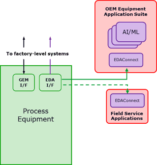 The EDA standards also include a provision for “built-in DCPs” (DCP = Data Collection Plan) which can be shipped with the equipment and protected from accidental deletion at the factory site. These DCPs could be crafted by the equipment supplier to directly feed whatever value-added applications the supplier chose to develop, whether these resided on a computer local to the equipment in the fab, on portable computers used by field service engineers to diagnose problems, or on remote cloud-based systems allowed to connect via secure EDA-defined URLs. This flexibility opens up a wide range of application types, from those that embed equipment-specific algorithms to generic Machine Learning frameworks… the possibilities are endless.