Industry News, Trends and Technology, and Standards Updates

Exposing Hidden Capacity through Material Tracking: Episode 2 in the “Models in Smart Manufacturing” Series

Posted by Alan Weber: Vice President, New Product Innovations on May 9, 2017 11:38:00 AM

“Do you know where your wafers are? Are you SURE?”

This adaptation of the famous public service announcement is as relevant for semiconductor process and industrial engineers as it was (and still is) for responsible parents. Given the ever-present productivity and profitability pressures in modern wafer fabs, it is essential to know the location and status of all product material at all times, because this information drives the scheduling and material delivery systems that provide competitive advantage for the world’s leading manufacturers. Until recently, material visibility at the lot/FOUP level was sufficient for this purpose, but this is no longer the case. 

Where_are_you.jpg

As production managers look for ways to squeeze more capacity out of their existing capital equipment, they realize that a deeper understanding of the wafer processing sequence within a particular tool type may provide opportunities to shorten the its overall lot processing time and increase the amount of material that can be processed simultaneously.  The first improvement results from identifying and eliminating unnecessary “wait” states* that individual wafers (or groups of wafers) may experience because of sub-optimal internal material handling, shared resource constraints, mis-calibrated subcomponents, poor recipe design, or a combination of these and other factors. The second improvement results from starting the next lot scheduled for a given tool as soon as all the wafers in the current lot have cleared the first stage of the process. This technique is sometimes called “cascading” or “continuous processing,” and applies to an increasing number of multi-chamber equipment types.

When applied to all the critical “bottleneck” tools in a factory, you can imagine what the resulting benefits would be for cycle time and capacity. Estimates of 3-5% improvement in these KPIs are not unrealistic.

Easy to say, right? But not so easy to implement? Perhaps not as daunting as you think…

The information required to track the precise location, movement, and status of individual wafers in semiconductor manufacturing equipment is most likely available for most equipment types in the form of “events” that chronicle the behavior of substrates, substrate locations, process chambers, aligners, wafer handling robots, and the other equipment components that affect wafer processing. What’s missing is a standard model that unifies this information across multiple equipment types, which would greatly simplify the data collection and analysis software required to implement a robust, generic material tracking system.

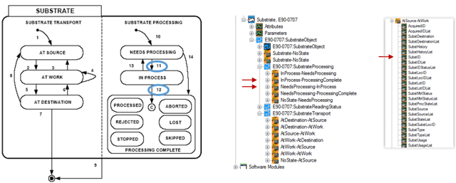
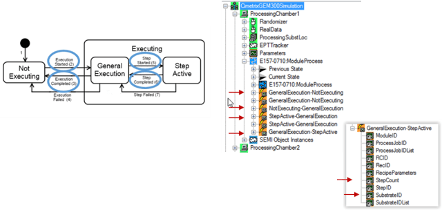
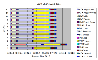
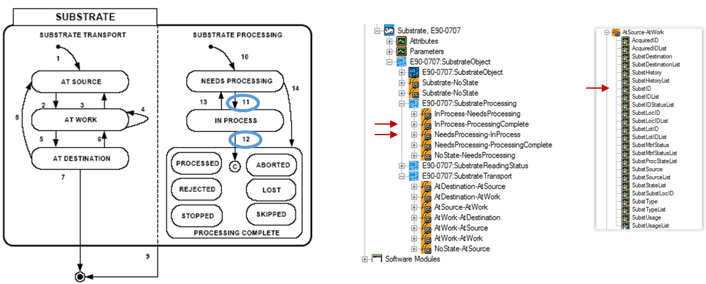
Here, too, the industry standards are actually ahead of today’s “state of the practice.” For example, the SEMI E90 “Substrate Management” and E157 “Specification for Module Process Tracking” standards define all the state machines, transition events, and associated context parameter data necessary to create a detailed Gantt chart of individual wafer movement and processing from start to finish, and allocate each contiguous time segment to its associated “active” or “wait” time element. The insights gained from this sort of visualization point directly to the opportunities cited above for improved tool control and factory scheduling.

Excerpts of these standards, a treeview representation of their respective models, and examples of the potential tracking displays are shown below.

Models_1.png

Models_2.pngModels_3.png

Models_4.png

Note that the SEMI E164 “Specification for EDA Common Metadata” calls for the inclusion of E90, E157, and a list of other GEM300 standards in the EDA equipment metadata model, so any E164-compliant equipment would directly and completely support such a material tracking application.

This article is only the second in the series recently announced in the Models in Smart Manufacturing Series Introduction posting – be sure to watch for subsequent postings that will expand on this theme.

We look forward to your feedback and to sharing the Smart Manufacturing journey with you.

*The list of potential “wait” states for semiconductor manufacturing has now been precisely defined and standardized as SEMI E168 “Specification for Product Time Measurement.” The standard also describes how they can be calculated using a specific set of standard material movement events commonly used in 300mm manufacturing equipment.

Topics: EDA/Interface A, Models in Smart Manufacturing series, Smart Manufacturing/Industry 4.0

Models in Smart Manufacturing Series – Introduction

Posted by Alan Weber: Vice President, New Product Innovations on Mar 24, 2017 11:30:00 AM

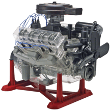
As a child I was an avid model builder—airplane models, trains, engines, cars, ships, even monsters (anyone remember “The Visible V8” and “The Creature”?)—anything I could get my hands on. At the time I didn’t reflect on the source of this fascination, but with the benefit of hindsight, it is clear that these models provided an interactive, tangible way to visualize, explore, understand, and enjoy the topics that were interesting to me. It was a way to enrich an otherwise intellectual activity.

Visible_V8.pngCreature.png

In fact, when Hurricane Carla ravaged the Texas coast and cut our electricity for 3 days, one of our luckier neighbors snaked an extension cord over the fence, which provided just enough power to run the refrigerator, a small black-and-white TV, and… you guessed it… my electric train. 

Model_train.png

More than four decades later, I still enjoy working with models, but in the high-tech manufacturing domain, they often operate in the reverse direction, providing a logical way to interact with and understand physical entities, like materials, fixtures, processes, devices, components, equipment, and entire systems. And as important as various model types have been throughout the relatively brief history of the semiconductor industry, they are increasingly an integral part of the “Smart Manufacturing” initiative that is sweeping a wide range of industries worldwide. 

The focus of my next few blog posts will be the specific models that are inherent in the communications interface definitions for manufacturing equipment, subsystems, and other devices that are expected to cooperate over the [Industrial] Internet of Things. Our first post in this domain almost a year ago introduced the notion that the metadata models called for in the latest generation of SEMI Equipment Data Acquisition (EDA) standards were already directly aligned with the Industry 4.0/Smart Manufacturing vision. This series goes into much more detail, showing how specific sections of the equipment models in the GEM and EDA standards directly support many of the factory monitoring, analysis and control applications that are essential for running a Smart Manufacturing enterprise (see Substrate Management example below).

substrate_management.png

Moreover, to the extent that the structure and content of these models can truly be standardized, their associated applications can be process- and supplier-independent, greatly reducing the development and support costs for the factory IT departments while providing useful capabilities for the production engineering and operations stakeholders.

To get a feel for the overall direction of this series, download the presentation "The Role of Models in Semiconductor Smart Manufacturing",  along with the transcript,  from the APC Conference held last October in Phoenix. Then watch for subsequent postings that address specific applications, from productivity (OEE) monitoring, material tracking, product traceability, process execution monitoring, and beyond.

We look forward to your feedback and to sharing the Smart Manufacturing journey with you.

Topics: Models in Smart Manufacturing series, Smart Manufacturing/Industry 4.0

Realizing Industry 4.0 with SEMI Standards: Right Here and Now

Posted by Alan Weber: Vice President, New Product Innovations on May 6, 2016 1:00:00 PM

IoT1.png

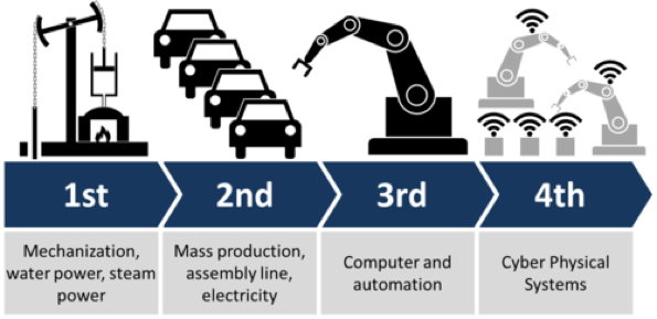
Since the concept was first articulated in 2011 by a German government-supported program promoting deeper integration of manufacturing software and hardware across the production value chain, the term “Industry 4.0” has gained recognition and momentum as the rallying cry for the 4th industrial revolution (see left Image by Christoph Roser at AllAboutLean.com). Wikipedia  summarizes it like this: “Industry 4.0 facilitates the vision and execution of a ‘Smart Factory.’ Within the modular structured Smart Factories of Industry 4.0, cyber-physical systems monitor physical processes, create a virtual copy of the physical world, and make decentralized decisions. Over the Internet of Things, cyber-physical systems communicate and cooperate with each other and with humans in real-time…” 

This definition may lead you to ask “What aspects of Industry 4.0 are truly revolutionary, and what technologies and tools are available today that would enable me to start building “Smart[er] Factories?” In this blog, I offer some potential answers to these questions that put the vision of Industry 4.0 within reach for automation practitioners familiar with the latest generation of SEMI Standards.  

IoT2.png

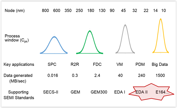
Semiconductor manufacturers have been collecting and using data from the equipment in their factories for decades. Throughout this period, device sizes and process windows have shrunk continuously according to Moore’s Law, and the SEMI Standards have evolved by necessity to support the insatiable demand for data exhibited by the process analysis and control applications that keep a modern fab running profitably (see left). The newest of these standards, the Equipment Data Acquisition suite (EDA, also known as “Interface A”), provides the power and flexibility to support a wide range of critical manufacturing applications and human users with ever-changing requirements; moreover, these standards can be deployed in a variety of system architectures without disturbing the “command and control” capabilities of existing factory systems.

“What does all this have to do with Industry 4.0?” To understand this, let’s look at the foundation of a “Smart Factory,” the collection of the many thousands of devices that might need to communicate over the so-called “Internet of Things.” 

We already see evidence that the availability of low-cost, low-power, networkable computing hardware will likely result in an explosion of “smart sensors” and other intelligent devices on the factory floor. However, as social scientists have observed over the millennia, groups of smart individuals don’t necessarily exhibit smart behavior in the aggregate, so what additional attributes must these devices possess to be good citizens of a collaborative, Industry 4.0 environment? How will these devices communicate effectively with one another? And what oversight will be required to ensure this communication achieves the ultimate manufacturing objectives?

As a starting point, I propose that each device, or manufacturing “thing,” at a minimum should be discoverable, autonomous, model-based, self-aware, communicative, and well-behaved. Depending on the role the device must play, it might also be self-monitoring, capable of defending itself (secure), and a consumer of data from other devices/systems as well as a provider. So defined, these devices would need a minimum of external monitoring and supervision (read “management overhead”) to perform their basic functions, but would rely on higher-level systems to provide specific objectives, instructions, and constraints (read “configuration, recipes, and limits”) for their operation in a given context and timeframe.

I realize that’s a lot to absorb at once, but now imagine that each of these devices could implement a subset of the services called for in the EDA standards, especially those defined in E120/E125/E164 (equipment modeling and standard metadata modeling), E132 (session management), and E134 (data collection management). Consider the collaboration among independent devices and systems this would enable…and ask yourself, how much closer to the vision of Industry 4.0 can you possibly get?

I hope the ideas above were useful…or at least thought-provoking. We’ll be developing this theme further in the coming months, but I wanted to use this blog as a conversation starter. We’d love to hear your feedback, so give us a call, or feel free to reach out to us.

Topics: Industry Highlights, Semiconductor Industry, EDA/Interface A, Smart Manufacturing/Industry 4.0

New Emerging Business and Technology Office

With the new year, comes a major new initiative for Cimetrix to grow the markets for its products.  The company used the transition to 300mm manufacturing to establish a leadership position for its current product portfolio in the semiconductor industry. However, the company is starting to have success expanding into adjacent vertical markets that includes disk drive, display, LED, and photovoltaic. The objective of this new initiative is for Cimetrix to leverage its experience, technology, and product portfolio gained in the advanced semiconductor manufacturing industry to expand the markets for Cimetrix products. We will be exploring new opportunities in our current adjacent markets as well as possible new markets such as SMT and electronic assembly.

Ranjan.jpeg

To head up this initiative, Ranjan Chatterjee has joined the company in the role of Vice President, Emerging Business and Technology Office. He will focus on extending and introducing Cimetrix’ portfolio of products into Industry 4.0 and Industrial Internet of Things (IIoT) initiatives by interfacing manufacturing equipment with big data and analytics tools. The data generated by devices connected via Cimetrix products can also be enlisted to bolster another methodology often used with lean manufacturing—Six Sigma. With the improvements in cloud and big data tools and infrastructure, one can use these methodologies on data with much bigger volume, velocity, and variety. This enables process control and a lack of variation of products. Processes can be monitored and corrected in real-time instead of inspecting machines merely at completion, and eventually this will help improve yields and reduce scrap. Specifically, manufacturers will need to establish a robust data infrastructure that works across the broader array of machines on the shop floor while breaking down protocol barriers so the machines can communicate effectively and in real time.

Manufacturers will also need to establish a bidirectional data flow so they are not only collecting information from equipment, but also pushing control back to the machines to optimize their usage. Manufacturers that can capture the right information, sift through it, and use it at the right time will be the ones that succeed.  Cimetrix intends to be a leader in enabling this vision. Ranjan’s decades of experience at Motorola and in the industry as a whole in software development, big data, cloud, process control, and lean manufacturing will enable Cimetrix to both adapt and develop products and partnerships to enable a robust ecosystem for a compelling solution.

Ranjan’s relationship with Cimetrix is not a new one as he is a former client. While at Motorola, Ranjan oversaw the development and deployment of a standards-based factory control system for SMT and assembly, which encompassed 24 factories around the world, and connected to over 20,000 pieces of equipment using the first generation of Cimetrix connectivity software. At that time, it was the leader in cell phone manufacturing and the largest purchaser of SMT equipment in the world. More recently, Ranjan has worked with companies developing and deploying systems using cloud technologies, big data analytics, and various modern technologies with a global software development team.

Ranjan is extremely excited to join the Cimetrix team as he sees many opportunities to leverage the latest cloud and big data analytics with Cimetrix core expertise and product portfolio into new markets for Cimetrix. He sees great potential for expanding Cimetrix in this new direction and we here at Cimetrix are looking forward to Ranjan leading the way.

If you are interested in discussing possible business opportunities and/or partnerships with Cimetrix with this new initiatives, please fill out our contact form to reach the Emerging Business and Technology Office.

Topics: Doing Business with Cimetrix, Investor News, Smart Manufacturing/Industry 4.0, Meet Our Team

SEMICON Europa 2015 Offers Insights into Upcoming Trends in the Semiconductor Industry in Europe

This week Cimetrix exhibited at SEMICON Europa 2015 along with about 400 other companies in the semiconductor industry in Dresden, Germany. The leading trade fair offered a chance for members of the industry to learn about new topics, information, and opportunities to help support and further develop the semiconductor industry across Europe.

An estimated 6,000 were in attendance at this SEMI-sponsored event. Some of the highlights of the three-day event were:

  • The Industry 4.0 Session: The term "Industry 4.0" has been established to describe the penetration of information science into manufacturing forming the next industrial revolution. The TechArena provided information about different aspects of this process.

  • The Emerging Research, Materials and Processes Session: The nanoelectronics research community is continuously exploring a range of new materials to enable further scaling of semiconductor devices and associated technologies, as well as many potential methods to create these materials with methods that allow utilization for future technology nodes. In this session several of these new materials and process developments were discussed by experts in their specific fields. Focus was on the unique properties of the materials or processes, what makes them specifically suitable for targeted applications, how they are characterized and/or how they can be fabricated. Among the topics that were presented were the newest developments for GaN processing, two-dimensional semiconductors devices and fabrication, metal organic frameworks as low-k materials, advanced memory materials such as FeRAM or MRAM Spintronics, and Selective Atomic Layer Deposition.

  • The Semiconductor Technology Conference (STC): This conference explored the efforts of our industry to ensure productivity enhancements for future advanced technology nodes, considering both a wafer size transition, and a continuation of current state of the art and smaller wafer sizes. Updates from around the world on wafer size transition activities were heard and there was a dedicated focus on “beam-based” metrology activities from METRO450 in Israel. SEMI invited their partners to share with attendees their insights, activities, and results in the preparation of future offerings of process equipment, materials, IT/fab automation systems, facilities and fab infrastructure, in order to rise to the challenge to ensure a continued economic manufacturing of state of the art semiconductor chips.

This year we exhibited as part of Silicon Saxony's Industrie 4.0 booth that consisted of about 40 kiosks representing companies with varying focuses within the industry. On Wednesday night, Silicon Saxony played host to all of the booth's exhibitors in a "Countries of Europe"-themed party. The event gave the Cimetrix team a chance to catch-up with friends and colleagues, and discuss new business opportunities. We'd like to thank Silicon Saxony for the great networking opportunity.

We are looking forward to SEMICON Europa 2016 in Grenoble, France next October and hope to see you there. If you didn't get a chance to meet with Cimetrix in Dresden this week and you would like to learn more about our complete line of factory connectivity and equipment control software solutions, please click here

Topics: Semiconductor Industry, Events, Smart Manufacturing/Industry 4.0