Industry News, Trends and Technology, and Standards Updates

The Giga Factory Minute Series Introduction: What to Watch for in 2019

Posted by Alan Weber: Vice President, New Product Innovations on Jan 17, 2019 11:05:00 AM

Gigafab-Minute-1We introduced the Giga Factory Minute concept last year to highlight the impact that standards have in orchestrating the entire manufacturing process, from releasing unpatterned wafers into the line (1:00 on the figure) to the shipment of good die to the downstream assembly/test facilities (12:00). This year, we’ll use this same diagram to identify important industry trends, technologies, events, or other items of interest to our subscribers. Since there are 12 “hours” on the diagram, watch for a posting every month related to the topic in that segment.

January 2019

Since this is January, we’ll focus on the more general topic of electronics manufacturing product materials, of which “wafer starts” is the specific material type that begins the 4-month journey through the wafer fab.

In the early days of the automated factory industry, there were only a few material form factors to deal with… even when you go all the way back to the raw silicon and forward to the finished electronic product. (You can see most of these on the “Sand to Systems” infographic here.)
However, now that semiconductors have found their way into virtually every major industry on the planet, from computers to entertainment to transportation to agriculture to wearables and even to “ingestibles,” the automated material handling challenges across this product diversity have exploded. And it’s only going to get worse. Red_smart_factory

You may not be responsible for handling exotic material types anytime soon, but understanding the role that equipment connectivity standards can have at the earliest steps in a Smart Manufacturing process is useful nevertheless. Give us a call if you’d like to know more about how these technologies can benefit your operations. 

Schedule a Meeting


Topics: Semiconductor Industry, Smart Manufacturing/Industry 4.0

SEMICON Korea 2019 is Coming up Next Week!

Posted by Kimberly Daich; Director of Marketing on Jan 15, 2019 10:27:00 AM

2019SEMICONKorea_468X60

Read now in Korean or below in English.

씨메트릭스는 이번 2019 년 SEMICON Korea전시회에서 귀사와 만날 수 있기를 바랍니다! 올해 우리는 부스 # C818에서 우리의 파트너인 링크제니시스와 공동으로 전시합니다. 전시회는 1 월 23 일부터 25 일까지 서울 코엑스에서 개최됩니다. 씨메트릭스는 장비 자동화와 통신 소프트웨어 관련 최고 기업으로서 한국뿐 아니라 글로벌 시장에서 동반자로 같이 일할 수 있는 여러분들을 만나고자 합니다.SEMICON Korea는 1987 년에 시작되어 대한민국의 반도체 산업가 그 성장을 같이 해왔습니다. 이번 전시회에서도 반도체 소재 및 장비의 모든 최신 기술을 선보일 예정입니다. 특별 프로그램 중에는 인공 지능 정상 회의 (AI Summit), AI 관련 새로이 창출된 기회를 진단해 볼 수 있는 자리와 반도체 업계 입장에서 인공 지능과 자동차의 부상에 따르는 시장을 이해하는 데 도움이되는 세미나, 차세대 혁신가들을 끌어 들이기위한 Workforce Development Seminar등이 있습니다. Smart Manufacturing 포럼은 우리 업계에 일어나고 있는 큰 변화와 커다란 기회에 대하여 모두가 함께 일하면서 무엇이 효과적이며 다음에 필요한 것이 무엇인지를 논할 예정이여서 많은 분들에게 인기가 있을 것으로 예상합니다.

씨메트릭스 제품이 여러분의 현안뿐 아니라 미래의 전략이나 Smart Manufacturing이라는 목표에 어떻게 도움이 될 수 있는지 자세히 알고 싶으시다면 전시회 기간 중 C818 부스를 방문하여 주시기 바랍니다. 웹 사이트를 통하여 언제든지 회의를 요청하실 수도 있습니다. 전시자에서 곧 봽기를 기대합니다! 

Meet with Us


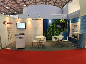
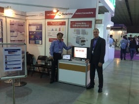
Cimetrix is heading to the 2019 SEMICON Korea show next week, and we hope to see many of you there! This year we are co-exhibiting with our partner Linkgenesis at booth #C818. The show will be at COEX in Seoul from January 23 – 25. We look forward to meeting with clients, prospects and colleagues to discuss new opportunities.

SEMICON Korea launched in 1987 and has been bolstered by the growing semiconductor industry in Korea. This exhibition will showcase all the latest technology in semiconductor materials and equipment. Some of the special programs include an AI Summit, examining new opportunities with AI implications, a Market Seminar to aid in understanding the rise of AI and automotive in the  industry, and a Workforce Development Seminar, aimed at drawing the next generation of innovators to the industry. A Smart Manufacturing forum is going to be popular as there are big changes and big opportunities for our industry as we work together to share what’s working and what is needed next.

If you would like to learn more about how Cimetrix products can help with your Smart Equipment and Smart Factory goals, please stop by booth #C818 during the show. You can also request a meeting any time on our website. We look forward to seeing you there!

Meet with Us


Topics: Semiconductor Industry, Doing Business with Cimetrix, Events, Smart Manufacturing/Industry 4.0

Cimetrix is gearing up for the 2018 SEMICON Japan show next week!

Posted by Kimberly Daich; Director of Marketing on Dec 4, 2018 4:19:00 PM

SCJapanシンメトリックスは、来週開催されるセミコンジャパン2018に向け、準備を進めています。今年も皆様にお会いできることを、楽しみにしております。Read now in Japanese or below in English.

今年弊社は、スマート・マニュファクチュアリング・エリアにブース(♯3493)を設置しており、弊社のスマート・マニュファクチュアリングのソリューション提案をご紹介しています。

また半導体産業エリアでは例年通り、長年弊社の代理店をお引き受け頂いておりますローツェ株式会社様(♯5507)、株式会社明電舎様(♯4626)と共同出展させていただいております。

今年もお客様、ソリューションをお探しの方々、また様々なパートナー様とお会いし、将来へ向けてのご協力のお話しをさせていただけることを、楽しみにしております。

SEMICON Japanが2018年に選んだテーマは、「今始まる成長と繁栄」(Dreams that Fuel Growth and Prosperity Start Here)です。日本は世界の半導体製造装置の3分の1、世界の半導体製造業界で使用されている材料の半分以上を供給しています。

SEMICON Japanは、日本と世界のエレクトロニクス製造サプライチェーン企業との関係をとりもつ素晴らしいイベントです。

SEMICON Japanには、スマート産業と半導体サプライチェーンを結ぶSMART Applications Zoneや、この関連産業界の新しい事業を紹介するイノベーションビレッジなど、いくつかの革新的な分野があります。また、世界的なネットワークを構築し、展示会を大いに盛り上げるパビリオンがいくつもあります。 

セミコン期間中に、ブースにお立ち寄り頂ければ、Cimetrix製品がスマートマニュファクチャリングにどのようにお役に立てるか、ご相談させて頂けると思います。またWEBミーティング等でもいつでもご相談頂けますので、お気軽にお申し付け下さい。会場でお会いできることを、楽しみにしております。

Meet with Us


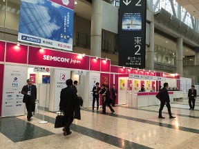
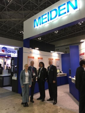
SCJapanCimetrix is gearing up for the 2018 SEMICON Japan show next week, and we hope to see many of you there! This year we will have a booth in the Smart Manufacturing Area (#3493) and we will also be co-exhibiting with Rorze (#5507) and Meiden (#4626) who have been our long-time distributors.  We look forward to meeting with clients, prospects and colleagues to discuss new opportunities.

The theme that SEMICON Japan has chosen for 2018 is “Dreams that Fuel Growth and Prosperity Start Here”. Japan supplies one third of the semiconductor manufacturing equipment and more than half of all the materials used by the global semiconductor manufacturing industry. As a result, SEMICON Japan is a great event to make connections with both the Japanese and global electronics manufacturing supply chain companies.

SEMICON Japan will feature several innovative areas including the SMART Applications Zone, which will connect SMART industries with the semiconductor supply chain, and an Innovation Village which is a place to showcase startups in this industry. There will also be several pavilions that generate a global networking energy and foster excitement for the show. 

If you would like to learn more about how Cimetrix products can help with your Smart Manufacturing goals, please stop by during the show. You can also request a meeting any time on our website. We look forward to seeing you there!

Meet with Us

Topics: Semiconductor Industry, Doing Business with Cimetrix, Events, Smart Manufacturing/Industry 4.0

The Gigafab Minute and SEMI Standards: A Modern Miracle

Posted by Alan Weber: Vice President, New Product Innovations on Oct 4, 2018 11:04:00 AM

Gigafab minuteEven for someone who has been in this industry since the days of the TI Datamath 4-function calculator and the TMS1100 4-bit microcontroller (yes, that’s been a LONG time – the movie Grease premiered the same year!), it is sometimes hard to grasp the scope and complexity of what happens in today’s leading-edge semiconductor gigafabs. In fact, the only way to comprehend the enormous volume of transactions that occur is to consider what happens in a single minute – this is illustrated in the infographic we have labeled “The Gigafab Minute.”* 


It’s amazing enough to think that a single factory can start 100,000 wafers every month on their cyclical journey through 1500 process steps… and have 99%+ of them emerge 4 months later to be delivered to packaging houses and then on to waiting customers. It’s quite another to realize that all of this happens continuously (24 x 7) and automatically. TMS1100-TIDatamath-image

“How is this possible?” you ask.

Well, a big part of the solution is the body of SEMI standards which have evolved since the early 80s to keep pace with the ever-changing demands of the industry. From an automation standpoint, many of these standards deal with the communications between manufacturing equipment and the factory information and control systems that are essential for managing these complex, hyper-competitive global enterprises.

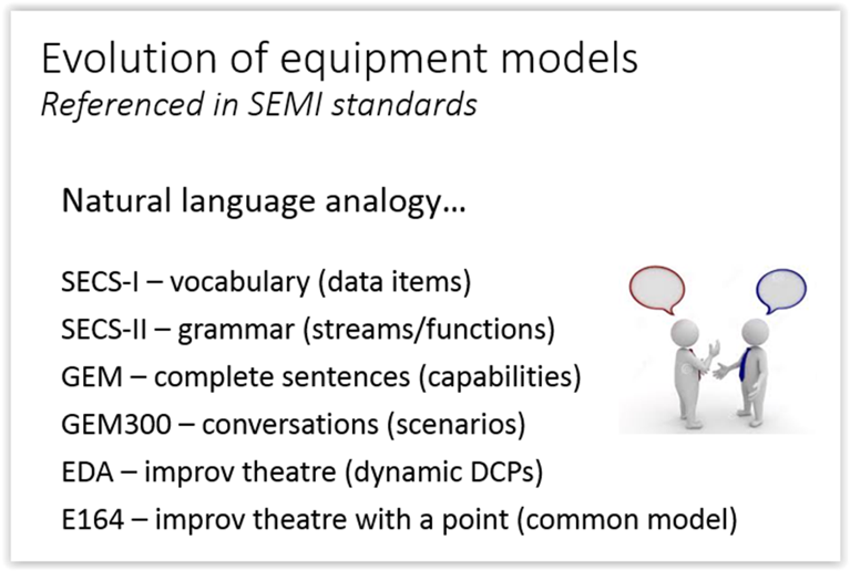
A significant characteristic of these standards is that they have been carefully designed to be “additive.” This means that new generations of SEMI’s communications standards do not supplant or obsolete the previous generations, but rather provide new capabilities in an incremental fashion. To appreciate the importance of this in actual practice, consider how the GEM, GEM300, and EDA/Interface A standards support the transactions that occur in a single Gigafab Minute. 

Starting at 1:00 o’clock on the infographic and moving clockwise, you first notice that 2.31 wafers enter the line. Of course, these are actually released in 25-wafer 300mm FOUPs (Front-Opening Unified Pod), but 100K wafers per month translates to 2.31 per minute. Since these factories run continuously, once the line is full, it stays full. And with an average total cycle time of 4 months, this means that there are 400K wafers of WIP (work in process) in the factory at any given time. This number, and the total number of equipment (5000+), drive the rest of the calculations. 

GEM (Generic Equipment Model) – SEMI E30, etc.

The GEM messaging standards were initially defined in the early 90s to support the factory scheduling and dispatching applications that decide what lots should go to what equipment, the automated material handling systems that deliver and pick-up material to/from the equipment accordingly, the recipe management systems that ensure each process step is executed properly, and the MES (Manufacturing Execution System) transactions that maintain the fidelity of the factory system’s “digital twin.” 

Every minute of every day, GEM messages support and chronicle the following activities: 240 process steps are completed (i.e., 240 25-wafer lots are processed), 300 recipes are downloaded along with a set of run-specific adjustable control parameters, and 600 FOUPs are moved from one place to another (equipment, stockers, under-track storage, etc.). For each of these activities, the factory’s MES is notified instantaneously.

GEM300 – SEMI E40, E87, E90, E94, E157

With the advent of 300mm manufacturing in the mid-to-late 90s, a global team of volunteer system engineers from the leading chip makers defined the GEM300 standards to support fully automated manufacturing operations. Starting at 5:00 o’clock on the infographic, the number of transactions per minute jumps almost 3 orders of magnitude, from the monitoring of 900 control jobs across 4000 process tools to the tracking of 360,000 individual recipe step change events. This level of event granularity is essential for the latest generation of FDC (Fault Detection and Classification) applications, because precise data framing is a key prerequisite for minimizing the false alarm rate while still preventing serious process excursions. In this context, more than 6000 recipe-, product- and chamber-specific fault models may be evaluated every minute.

Simultaneously, the applications that monitor instantaneous throughput to prevent “productivity excursions” and identify systemic “wait time waste” situations depend on detailed intra-tool wafer movement events. In a fab with hundreds of multi-chamber, single-wafer processes, 75,000 or more of these events occur every minute. gantt-chart-cycle-time

EDA (Equipment Data Acquisition) – SEMI E120, E125, E132, E134, E164, etc.

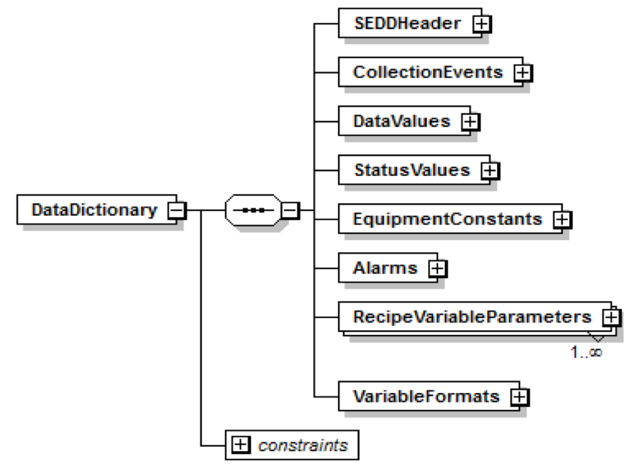
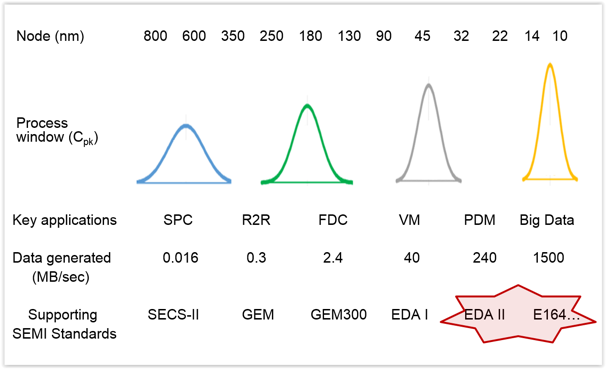
Rounding out the SEMI standards in our example gigafab is the suite of EDA standards which complement the command and control functions of GEM/GEM300 with flexible, high-performance, model-based data collection. The EDA standards enable the on-demand collection of the volume and variety of “big data” required from the equipment to support the advanced analysis, machine learning, and other AI (Artificial Intelligence) applications that are becoming increasingly prevalent in leading semiconductor manufacturers. As EUV (Extreme Ultraviolet) lithography moves from pilot production to high-volume manufacturing at the 7nm process node and beyond, the litho process area will become a major source of process data by itself, generating 10 GB of data every minute. This is in addition to the 100 GB of data collected from other process areas. graph-and-equipmentfolder

The End Result

The final wedge (12:00 o’clock) in our infographic highlights the real objective – which is producing the millions of integrated circuits that fuel our global economy and provide the technologies that are an integral part of our modern way of life. Assuming a nominal die size of 50 square mm (typical of an 8 GB DRAM), the 2.31 wafers we started at 1:00 o’clock result in almost 3200 individual chips. But none of this would be possible without the pervasive factory automation technology we now take for granted. So, as you finish reading this posting on whatever device you happen to be using, take a micro-moment to acknowledge and thank the hundreds of standards volunteers whose insights and efforts made this a reality!

Red_smart_factory-TWYou may not be responsible for running a gigafab anytime soon, but the SEMI standards used in this setting are no less applicable to any Smart Manufacturing environment. Give us a call if you’d like to know more about how these technologies can benefit your operations for many years to come. 


You can see this infographic and much more in the Cimetrix Resource center.

Resources

 *The Gigafab Minute was inspired by an analogous explication of the scope and impact of today’s Internet from Lori Lewis and Chadd Callahan of Cumulus Media, and published on the Visual Capitalist web site (http://www.visualcapitalist.com/internet-minute-2018/)

Topics: Industry Highlights, SECS/GEM, Semiconductor Industry, Smart Manufacturing/Industry 4.0

SEMICON West 2018 Standards Committee Meeting Updates

Posted by Brian Rubow: Director of Solutions Engineering on Jul 18, 2018 12:30:00 PM

SEMI-member

During the SEMICON West exhibition in San Francisco this past week (July 9-10), the North American Information & Control Committee and its Task Forces met to continue SEMI standards development. Here is a brief summary of the proceedings.

The GEM 300 task force, in addition to reapproving E90, also approved minor title changes to the E39, E39.1, E40 and E40.1 standards. Each SEMI standard must be revised or reapproved to avoid becoming inactive. A few years ago, SEMI changed regulations that mandate that each standard declare its classification, such as a “guide” or “specification”. Since then the task force has been slowly correcting the titles. The E37.1 standard is in the middle of such classification, but has been riddled with reapproval complications due to minor concerns and some needed corrections in the standard. The ballot to make these corrections, 6349, failed for the second time at SEMICON West. The ballot will be slightly reworked and resubmitted for another round of voting. Another ballot, 6348 proposed to clean up the GEM E30 standard, to improve its readability and to bring the standard in conformance with current SEMI regulations and its current style guide. The forefront of the discussions was surrounding the confusing use of acronyms DVNAME, DVVAL, SVV and other such acronyms where the meaning and use of the acronyms was confusing to new readers. The 6348 ballot also failed, but hopefully the task force is progressing towards reaching an agreement. One major challenge is that ballot 6348 is a major revision ballot, where the entire specification is opened up for review and scrutiny, as opposed to line item ballots where only specific sections of a standard are modified.

Finally, and most exciting is ballot 6114B; a revision to the SECS-II E5 standard. The ballot proposed a set of new messages for transferring any large items between a host and equipment. Typically, one item in a message is limited to about 16.7 MB. The new messages are specifically targeting the transfer of equipment recipes, but the messages are written generic enough so that anything else can be transferred, too. The new messages support two styles of item transfer. Either the item can be transmitted in a single message, or broken into parts for transfer with the expectation to be concatenated by the recipient. Or the item can be transmitted in multiple messages, broken into parts with each part sent in a separate message and the same expectation to be concatenated by the recipient. An item is identified by its “type”, “id” and “version”. The messages are intended to resolve current issues with recipes where some equipment suppliers are using recipes that surpass 16.7 MB. And the messages open the door to be used by other SEMI standards and to be customized for specific applications. After passing this ballot, the task force intends to make the messages part of the GEM standard. Even though the ballot 6348 failed, the task force seems to have finally reached consensus on the message formats and continues to work out minor details.

The DDA Task Force continues to work on the next version of the Equipment Data Acquisition (EDA) standards. In the latest cycle of voting, changes were proposed to E138 (ballot 6336), E134 (ballot 6335) and E132 (ballot 6337). Although one part of E134 passed, most of E134 failed and the other ballots failed. All of the failed ballots will be reworked and resubmitted for voting. Additionally, during the task force meeting additional proposed changes were reviewed and discussed. The task force continues to make plans to move from HTTP 1.1 and SOAP/XML to HTTP 2.0 and Protocol Buffers. Specifically, the plan is to recommend using gRPC. Testing done to date indicated an 18 times performance improvement and significant bandwidth reduction. The task force also discussed changes to simplify the equipment model metadata handling. Finally, Cimetrix proposed the implementation of a new method of data sampling designed for higher data collection frequencies. The current trace data collection messages, while very effective for speeds up to maybe 80 Hz, become inefficient when trying to collect data at even faster rates. The concept is called a “cached data sample” where the equipment collects the data at a specified frequency and then reports the data in an array syntax. When using HTTP 2.0 and Protocol Buffers, this will be an especially efficient format expected to allow much higher frequencies.

The client specifies the data collection frequency as well as the reporting frequency. For example, a client might specify a frequency of 10 kHz and a reporting frequency of 1 s, where 10,000 data samples would be reported each second. Such proposal if accepted, combined with the faster Protocol Buffer, will open the door for a number of new data collection applications.

A lot of people are wondering when EDA freeze III will be done. Probably not until late next year. How soon this happens mostly depends on how efficiently task force members provide feedback on the ballot drafts.

Subscribe to our blog in the upper right corner of this page to be sure not to miss that or any of my future updates on the North American Information & Control Committee.

Topics: Industry Highlights, Semiconductor Industry, EDA/Interface A, Events

SEMICON West 2018 - Smart Manufacturing Pavilion Speech by Alan Weber

Posted by Kimberly Daich; Director of Marketing on Jul 11, 2018 2:02:00 PM

SEMICON West_BS_RGB_vert-187776-editedCimetrix is here at SEMICON West 2018 and we're excited to be a part of the first Smart Manufacturing Pavilion in the South Hall. We hope you've been able to drop by and hear some of the great speeches including our own experts Alan Weber, VP New Product Innovations and our VP & GM Smart Factory Business Ranjan Chatterjee with Dan Gamota (VP Digital Engineering Services) at Jabil.

Alan Weber's presentation is now available online. The topic he chose is "Making Smart Manufacturing Work: The Stakeholder-driven Requirements Development Process".

An important maxim of performance management is “You get what you measure.” This is largely true whether you are talking about employees, organizations, processes, time management, sports teams, or – to highlight a current global industry topic – Smart Manufacturing.

semi-west-alan-2018-3The question now becomes “How DO the industry’s leading manufacturers ensure the equipment they buy will support their Smart Manufacturing objectives?” This presentation explains how the careabouts of key stakeholder groups are “translated” into specific equipment automation and communications interface requirements which can then be directly included in the equipment purchasing specifications. As more semiconductor manufacturing companies take this approach, effectively “raising the bar” for the entire industry, the collective capability of the equipment suppliers will increase in response, to everyone’s benefit.

Through several interviews with leading manufacturers over the past 18 months, we discovered that the best way to accomplish this is through a focused, interactive questionnaire process. By asking very specific questions about people’s daily tasks, problem areas, expectations, success criteria, and other items of constant concern, we can take a generic automation purchase specification outline and generate a complete, factory-specific set of automation and communications interface purchase specifications in a matter of days. This is time well-spent when you consider the value and volume of equipment potentially affected… and the opportunity cost of not having these requirements clearly expressed.

If the above discussion triggers the question “I wonder if our equipment automation purchase specs are sufficient to address the Smart Manufacturing challenges we’ll face in the next few years?” this presentation will interest you. Taking its lessons to heart may be the most important next step you take in formulating you own company’s Smart Manufacturing implementation roadmap.

Get Alan Weber's SEMICON West presentation now!

Download Presentation

Topics: Industry Highlights, Semiconductor Industry, Doing Business with Cimetrix, Events

SEMICON West 2018 Pre-Show

Posted by Kimberly Daich; Director of Marketing on Jul 5, 2018 12:29:00 PM

SEMICON West 2018 Beyond SmartSEMICON West 2018 is fast approaching and the Cimetrix team is gearing up for a great show.  The show runs from July 10th – 12th at the Moscone Center in San Francisco and we’re looking forward to meeting with all our present and future clients.

This year SEMICON West is unveiling the new Smart Manufacturing Pavilion to showcase the entire manufacturing process from silicon to systems, including Front End, Back End and PCB Assembly. Cimetrix is excited to announce that we are a sponsor and will be participating in the Smart Manufacturing Pavilion showcase, both as part of the Front End segment as well as in the PCB Assembly area.

The Smart Manufacturing Pavilion includes a “Meet the Experts Theater” featuring presentations from two of our own Cimetrix thought leaders.  Alan Weber will present “Making Smart Manufacturing Work: The Stakeholder-driven Requirements Development Process” on Wednesday, July 11th at 11:00 am. This process has already been used successfully to support the significant growth of SEMI EDA standards usage in Asia, but is equally relevant for a wide range of related Smart Manufacturing technologies.

Later on Wednesday afternoon at 3:00 pm, Ranjan Chatterjee and Dan Gamota of Jabil will present “Convergence of Technologies and Standards Across the Semiconductor, SMT and OSAT Segments.” 

Cimetrix will be exhibiting at booth #1122 in the South Hall, just a short walk from the Smart Manufacturing Pavilion. Stop by our booth or find us at the Pavilion to talk to our experts about your specific needs. We will have onsite product demonstrations as well as information about our company available.  You can also schedule in advance a time to meet with us at the show by filling out a quick form with your meeting request.  

Schedule a Meeting

See you at SEMICON!

Topics: Semiconductor Industry, EDA/Interface A, Events, Smart Manufacturing/Industry 4.0, SMT/PCB/PCBA

CCF为实施工厂自动化提供了一条捷径: CCF Gives an Easy Way to Implement Factory Automation

Posted by Yufeng Huang; Software Engineer China on May 10, 2018 11:37:00 AM

Yufeng Huang of Cimetrix China, talks about Equipment Control in the factory. Read now in Chinese or below in English.

在和半导体设备制造公司的接触中我们遇到这么一个尴尬的问题,很多懂得设备控制的优秀软件工程师对于GEM,GEM300和EDA标准不是很有经验。这些公司往往是在设备在实验室研发成功,准备产业化送入客户工厂时发现设备没有实现或只有部分实现GEM/GEM300标准,尤其是当客户工厂要求EDA(Interface A)通信接口的时候,这些设备制造商的软件工程师往往一脸茫然,不知道如何在短时间内开发出完全遵循GEM/GEM300/EDA标准的软件。

对于大多数设备公司而言,限制于有限的人力、财力资源,公司很难聘请到足够多富有经验的工厂自动化软件工程师开发自己的GEM/GEM300,甚至EDA软件模块。另外一个棘手的问题是我们发现很多软件工程师不是特别有意愿加入到半导体行业,而是选择比较热门的互联网、游戏,手机App等软件行业。纵观半导体工厂自动化软件市场,虽然已有多家公司提供GEM/GEM300/EDA的软件开发包(SDK),但软件工程师仍旧需要掌握一定的工厂自动化基础知识才能着手编写软件集成代码。工厂自动化涉及大量SEMI标准,譬如GEM标准大概有450页文档,包括E4,E5E30E37,E37.1,E172,E173,GEM300标准大概有280页文档,包括E39,E40,E87,E90,E94,E116,E157,E148,而更为复杂的EDA标准大概480有页文档,包括E120,E125,E128,E132,E134,E138,E164,对于大多数非专业的工厂自动化软件工程师而言,工厂自动化软件的集成工作是一件极其繁琐而艰难的任务。


Cimetrix Control FrameworkTM (CCF)
是基于微软.Net技术的设备自动化控制软件框架,该软件不仅为设备制造厂商提供了监督控制和生产控制框架代码,而且完全实现了GEM/GEM300/EDA标准。借助CCF软件平台,软件工程师无需深刻掌握工厂自动化的所有SEMI标准,就能轻松变身为工厂自动化开发专家。CCF软件框架内的工厂自动化模块基于Cimetrix公司的CIMConnect,CIM300,CIMPortal Plus三个独立的软件开发套件(SDK)实现,分别对于实现GEM,GEM300,和EDA标准。全球任意一家300mm的芯片制造工厂都有安装了CIM300软件的设备运行,在支持EDA数据采集的工厂都有安装了CIMPortal Plus软件的设备运行。CCF软件框架将所有工厂自动化的开发工作交给Cimetrix公司来完成,设备软件工程师可以把更多的时间花费在如何设计自己的设备控制软件上。

在CCF框架下,CIMConnect/CIM300/CIMPortal Plus的底层API函数都被很好作了封装,软件工程师只需通过CCF框架提供的函数或接口就能轻松实现和工厂主机程序的所有GEM/GEM300标准。实现EDA标准的一个重要任务是创建一个支持分层次结构的设备模型,以及按照标准生成XML数据,此外生成的模型还需满足E164标准。在CCF软件初始化运行时会动态生成设备模型,软件工程师几乎不需要书写EDA代码,设备即可很好的遵循EDA标准。lego brick building is like CCF

采用CCF软件框架降低设备控制程序和工厂自动化程序的开发难度和开发周期,但并不意味着我们的客户一定得推翻自己已有的软件平台或已经测试过的稳定代码。CCF是一个提供源代码的完全开放的自动化控制程序框架,你可以将CCF理解成一个已经拼好的乐高玩具,用户既可以将自己的代码模块集成到CCF中,也可以挑选部分CCF功能模块并将其转移到用户自己的框架中。我们用户将CCF中工厂自动化模块(包括GEM/GEM300/EDA)搬迁到自己的程序框架中,在保证完全遵循工厂自动化诸多SEMI标准的同时,对用户已有程序的影响非常小。

得益于CCF框架的完全开放性,像玩乐高积木一样,软件工程师可以轻松享受自由裁剪自己想要的控制系统框架带来的乐趣,这是其他任何一家提供设备控制软件框架程序的公司都很难做到的一件事情。

在未来几年,越来越多的工厂往智能生产制造的方向发展,由此对数据的需要越来越高,EDA标准越来越成为工厂主流的数据采集方法,CCF无疑成为了设备制造商更快更好实现各种工厂自动化标准的最佳武器。 


We encountered an interesting issue when working with semiconductor equipment manufacturing companies. Many excellent software engineers who know equipment control are not very experienced with the GEM, GEM300, and EDA standards. Sometimes after equipment is successfully developed in the laboratory and before the equipment is shipped to the factory, we discover that the equipment did not implement or only partially implemented the required GEM/GEM300/EDA standard. This is especially prevalent when the factory requires the EDA (Interface A) communication interface. Equipment software engineers sometimes do not know how to develop software that fully complies with GEM/GEM300/EDA standards in a short period of time.

For most equipment companies with limited human and financial resources, it is difficult for the company to have the resources to develop their own GEM/GEM300/EDA software. Another issue is that we have found many of the more experienced software engineers are more interested in high-profile  internet, gaming, mobile phone apps and other software industries rather than the lower profile semiconductor industry.  Although many companies in the semiconductor factory automation software market have provided GEM/GEM300/EDA software development kits (SDKs), software engineers still need to master certain basic knowledge of factory automation to start writing software integration code. Factory automation involves a large number of SEMI standards. For example, the GEM standard has about 450 pages of documents, including E4, E5, E30, E37, E37.1, E172, E173. GEM300 standards have about 280 pages of documents, including E39, E40, E87, E90, E94, E116, E157, E148. The more complex EDA standard has about 480 pages, including E120, E125, E128, E132, E134, E138, E164. For less experienced factory automation software engineers, the integration of automation software can be an extremely tedious and difficult task.

Cimetrix CIMControlFrameworkTM (CCF) is an equipment automation control software framework based on Microsoft .Net technology. This software not only provides equipment manufacturers with supervisory control and equipment control framework code, but also fully implements the GEM, GEM300 and EDA standards. With the help of the CCF software platform, software engineers can easily turn into factory automation development experts without having to master all the factory automation SEMI standards. The factory automation components within the framework of the CCF software are based on CIMConnect, CIM300, and CIMPortal Plus, three independent software development kits (SDKs) from Cimetrix for the implementation of the GEM, GEM300, and EDA standards, respectively. All 300mm chip manufacturing factories in the world have equipment installed which uses CIM300 software. Any factory requiring EDA data collection has equipment installed that uses CIMPortal Plus software. With the CCF software framework, Cimetrix has already done the work of integrating all factory automation into the framework. The equipment software engineer can spend more time on how to develop their own equipment control software.

Under the CCF framework, the underlying API functions of CIMConnect/CIM300/CIMPortal Plus are well encapsulated. Software engineers can easily implement all the GEM/GEM300/EDA standards of the factory host program through the functions or interfaces provided by the CCF framework. An important task in implementing the EDA standard is to create an equipment model that supports hierarchical structures and generate XML data in accordance with standards. In addition, the generated model must also meet the SEMI E164 standard. The equipment model is dynamically generated when the CCF software is initialized. The software engineer needs to do very little to have an equipment control application that is fully compliant with the EDA standard.lego brick building is like CCF

The use of the CCF software framework to reduce the difficulty and development cycle of equipment control programs and factory automation programs does not mean that our clients must replace their existing software platforms or stable code that has been tested. CCF is a fully open automation control program framework that provides source code. You can think of CCF as a LEGO toy that has been put together. Users can either integrate their own code modules into CCF or select some of the CCF functional modules and transfer them to their own framework. Our clients can reuse the factory automation modules (including GEM/GEM300/EDA) in CCF in their own program frameworks. While ensuring that all SEMI standards for factory automation are fully complied with. The impact on the user's existing programs is minimal.

Thanks to the complete openness of the CCF framework, like LEGO bricks, software engineers can easily enjoy the freedom of tailoring the control system framework that they want. It is hard for any company that provides an equipment control software framework program to implement such a rich library of functions. 

In the next few years, more and more factories will move in the direction of smart manufacturing. As a result, the demand for data is getting higher and higher. EDA standards are increasingly becoming the factory's mainstream data collection method. CCF will undoubtedly become the best weapon for equipment manufacturers to quickly and completely implement the various factory automation standards.

Topics: Industry Highlights, SECS/GEM, Semiconductor Industry, Equipment Control-Software Products, Cimetrix Products

Cimetrix has a Strong Presence in Europe: Wrap-up of SEMICON Europa and Productronica 2017

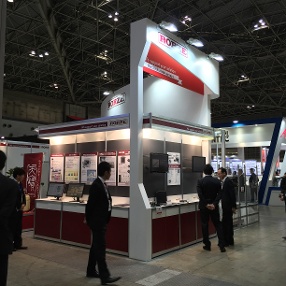
Prod_wrap_5.pngCan you think of a better place to spend time with customers and partners than Munich, Germany during Productronica and SEMICON Europa trade fairs? SEMICON Europa has had dwindling attendance in the past few years, even in a hot semiconductor market, so SEMI decided to combine with the robust Productronica for 2017.  It was a great decision.  This trade fair had 8 full and busy halls as a result; with high spirits from all attendees.  Four of the Productronica halls were dedicated to the SMT industry (Surface Mount Technology) which is part of what we call Electronics Assembly.  This industry is wrestling with moving to Smart Manufacturing and Industry 4.0.  What better way to learn than to have SEMICON Europa next door?  SEMICON Europa occupied 1.5 halls filled with many of our current customers. 

Prod_wrap_6.jpg

Cimetrix decided to place our booth in one of the four SMT halls because we have a lot to offer the SMT industry in their migration to Smart Manufacturing.  We had many visitors and discussions on how Cimetrix can help.  There are a variety of ways used in SMT to gather equipment data including older “one way” standards, GEM, and several proposed new standards and our 25+ year heritage in semiconductor equipment automation ideally positions Cimetrix to help customers think through these options.  We also brought extra staff to the show so we could spend time in the SEMICON Europa halls having scheduled meetings with our major European equipment suppliers and factories.  Several new opportunities were brought to our attention and updates/planning for 2018 were discussed. 

By far, the dominant theme at the show was Industry 4.0 and Smart Manufacturing.  There were many excellent presentations in the Tech Arenas; and almost every booth had posters on the move to Smart Manufacturing.  Of note were presentations by Dr. Jan Rothe from GLOBALFOUNDRIES and Jorg Richstein from Jabil discussing their automation plans for SMART Manufacturing; and Dr. Martin Schellenberger from Fraunhofer with a comprehensive set of steps to help companies understand Smart Manufacturing and the steps to get there. 

Prod_wrap_8.png

As a company that focuses on helping manufacturers achieve their automation goals, it is hard not to come away from Munich excited about the next 5 years in electronics manufacturing. 

Prod_wrap_4.pngProd_wrap_7.jpg


Topics: Semiconductor Industry, Doing Business with Cimetrix, Events

North America SEMI Standards Meeting Fall 2017 Recap

Posted by Brian Rubow: Director of Solutions Engineering on Nov 22, 2017 11:00:00 AM

semi.png

The SEMI North American Information & Control Committee meetings were held in Milpitas, CA at SEMI headquarters. The following activities might be important for Cimetrix customers and employees.

The DDA Task Force has officially kicked off the development of the next EDA standards, already deemed “Freeze 3” by many. Several ballots have been authorized for creation and voting early next year. This includes ballots to modify E125, E132, E134 and E138, which includes many of the core EDA standards. Additional work is also planned for E164. Most of the changes are expected to be straightforward, with a few corrections, clarifications and new features that various SEMI members have requested. E125 is probably the biggest proposed change in this set, where new messages will be added to provide the list of all parameters and the list of all events. Then the equipment nodes in the model will always reference parameters and reference events. This should clarify some of the confusion surrounding parameter definitions and parameter references.


By far, the longest discussion was surrounding the biggest decision of all. Currently, the EDA standards are using HTTP/1.1 for message transfer and SOAP/XML for message body. This means that the EDA standards are text based. At the time of EDA development, this seemed to be the best internet technology for data collection. Today, HTTP/1.1 is out of date. More recently, advances have been made in internet technology for sharing data in a binary format. The biggest advantage of transferring data in a binary message format is message efficiency. A binary message generally will be about 15 to 20 times smaller than text based messaging. This means less load on the equipment that publishes EDA data, much less load on the network and less load on the subscribing EDA clients. Many alternatives were discussed including WebSockets, HTTP/2, and even HSMS. It was discussed whether to stick with a text based protocol and use compression or move to a binary protocol. Data was presented from a DDA Task Force member regarding a performance comparison between HTTP/1.1 with text messages (like EDA today), HTTP with binary messages, HTTP/2 with SSL, WebSockets with binary messages and WebSockets with SSL. The test results showed binary messaging to be allow 25 times more data collection than the current HTTP/1.1 technology. Ultimately, it was decided that moving to a binary protocol was the right strategic direction.

Another point of discussion was how to implement binary messaging. Google has developed the Protocol Buffer technology. Specifically, we looked at version 3 called “proto3” which defines a notation for establishing binary messages. They have also published open source code gRPC in various software programming languages that implement the binary encoding and decoding for the Protocol Buffer technology and HTTP/2. This seems to be today’s best technology for binary web services. The DDA Task Force is in the process of developing a ballot to propose the adoption of this technology for the EDA messages. If approved, this would be the foundation of freeze 3 communication and a vast improvement.

In Japan, the Information & Control Committee recently created a DDA task force. The leader, Mitch Sakamoto from company ZAMA is coordinating with the North American DDA task force. Similarly, the DDA task force leaders in Korea are also working closely with North America. The Freeze 3 EDA development really is emerging as a worldwide coordinated development. The world-wide cooperation and coordination is much stronger and cohesive than the development was for Freeze 1 and Freeze 2.

The GEM 300 task force passed a ballot approving the use of SECS Message Notation (SMN) for GEM implementations. SMN could already be used anyway, but adding this to the GEM standard makes its use more official. This means that messages can be logged and documented using SMN.

The GUI task force continues to move along with planned improvements for the E95 standard. This including modernizing the graphics in the standard, updating the text and most importantly having the standard include the adoption of small screen devices as an equipment HMI. The new E95 standard will be a major revision standard.

In Korea, several ballots continue to be developed and reworked. This includes an update to the E87 carrier management services standard to allow more precise reporting when carrier approach the completion state. This includes an update to the E142 wafer map handling standard with new features in the schema file. Additionally, they are working on an equipment generic counter standard, which establish standardized methods for equipment to “count” things that happen on the equipment. This proposed specification is a favorite of mine personally. It is a clever way to recognize that it is important to count things on every equipment such as the number of times a vacuum has a been cycled, the number of times a nozzle has been used, the number of times a user has logged in, the number of times a robot has moved a substrate, the number of times an equipment has been restarted. It could be anything and it could be very different on two types of equipment. Collecting such data in a generic, natural way facilitates predictive maintenance; a key to minimizing factory equipment downtime.

Topics: Industry Highlights, Semiconductor Industry