Industry News, Trends and Technology, and Standards Updates

Thinking Ahead: Why would I want to buy EDA client libraries for my equipment?

Posted by Alan Weber: Vice President, New Product Innovations on Nov 11, 2020 11:30:00 AM

Background and Audience

Over the past several years, I have written numerous blog postings heralding the benefits of the SEMI Equipment Data Acquisition (EDA, also known as Interface A) standards, promoting their adoption by 300mm wafer fabs around the world, explaining how to develop robust purchase specs to ensure the interfaces delivered by the equipment suppliers meet the fab customers’ expectations, describing how the various components of the standards work together and the importance of the embedded equipment model, and finally explaining how to run compliance and performance tests on an EDA interface to validate its fitness for production use. The target audience for most of these postings has been the factory users, for they are the ones who increasingly depend on detailed equipment and process data to profitably run their enterprises.

By contrast, this posting is aimed at the equipment suppliers who are looking to increase the value of their product families by augmenting their hardware offerings with software capabilities that only they are uniquely qualified to provide.

This is not a new idea. Several major equipment suppliers have offered so-called “Equipment Engineering Systems (EES)” products as companions for their equipment over the years, providing applications like Fault Detection and Classification (FDC), production monitoring, maintenance management, local repositories for diagnostics and field support, and other capabilities that leveraged deep domain knowledge of the equipment. However, these systems necessarily relied on private interfaces to the equipment for their data, such as an additional network connection, direct access to the file system, or other mechanisms. And from the fab’s perspective, these constituted yet another piece of infrastructure to maintain.

Now there’s EDA: a key enabler for value-added equipment applications

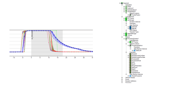
Since the SEMI EDA standards are inherently multi-client, a single EDA interface can support not only the factory information and control systems that depend on equipment data, it can also provide whatever information a supplier-specific application may need as long this data is represented in the equipment metadata model. Since that model is designed by the equipment suppliers as a fundamental component of the EDA interface, they can choose to put as much information in these model as they want, possibly well beyond that required by the fab customers’ purchase specifications. In fact, these models could be used to implement the diagnostic logging capability that suppliers usually build into their equipment for their own use, but without requiring custom software to read and interpret that information. See the figure below for an example of such a configuration.

EDA-Equipment-1The EDA standards also include a provision for “built-in DCPs” (DCP = Data Collection Plan) which can be shipped with the equipment and protected from accidental deletion at the factory site. These DCPs could be crafted by the equipment supplier to directly feed whatever value-added applications the supplier chose to develop, whether these resided on a computer local to the equipment in the fab, on portable computers used by field service engineers to diagnose problems, or on remote cloud-based systems allowed to connect via secure EDA-defined URLs. This flexibility opens up a wide range of application types, from those that embed equipment-specific algorithms to generic Machine Learning frameworks… the possibilities are endless.

What all these approaches have in common is a standard EDA client capability that can establish a session with the equipment, activate Data Collection Plans, and receive the ensuing Data Reports. The EDAConnecter within the Cimetrix Sapience platform provides all these features and more in a lightweight set of .NET libraries which can be deployed wherever they are needed to consume EDA data.

Conclusion

More and more semiconductor factories are requiring EDA interfaces with their new equipment purchases with highly prescribed equipment models and demanding performance criteria. From the equipment supplier’s perspective, these requirements have been viewed as a source of additional cost, with all the benefits accruing to the factory customers. But it doesn’t have to be that way…

Why not take advantage of this interface to offer additional value using a standards-based approach? This just might be an idea whose time has finally come. If you agree, give us a call – we can help you make it happen!

Topics: Industry Highlights, Semiconductor Industry, EDA/Interface A, Doing Business with Cimetrix, Standards

Semiconductor Backend Processes: Tracking Process Execution

Posted by Alan Weber: Vice President, New Product Innovations on Sep 30, 2020 11:45:00 AM

Background

semi-e157-pic1

Previous blog posting in this series have discussed the rationale for using SEMI’s GEM, GEM 300, and related automation standards in semiconductor backend factories, and pointed out that the specific adaptations required for the various backend equipment types are one of the focus areas for the SEMI Advanced Backend Factory Integration (ABFI) Task Force. In this posting, I will deal specifically with the benefits that can be realized by using the E157 Process Module Tracking standard in a backend factory context.

Since none of the backend material transformations are implemented in what front end experts would consider a “process chamber,” this may seem like an unlikely fit. Moreover, the velocity of backend processes seems contrary with the typical front end recipe execution paradigm. Finally, the lack of distinct substrate locations for some of the processes makes it difficult to know precisely when the process begins and ends for the affected material in some cases.

Regardless of these challenges, the requirements for single device traceability that include knowing the exact process conditions that a device was exposed to at every moment in its manufacturing life cycle (including the backend) argue for use of this standard wherever possible.Since none of the backend material transformations are implemented in what front end experts would consider a “process chamber,” this may seem like an unlikely fit. Moreover, the velocity of backend processes seems contrary with the typical front end recipe execution paradigm. Finally, the lack of distinct substrate locations for some of the processes makes it difficult to know precisely when the process begins and ends for the affected material.

SEMI E157 – Process Module Tracking

The purpose of SEMI E157 is “to define a standard equipment capability to report process-related data to the factory system… the activities of a processing location (i.e., process module) that are related to the execution of a recipe.” The standard further states that “the collection of process data during recipe execution is important to today’s semiconductor factories to support various applications that help optimize equipment processes, finished product quality, yield, and overall factory performance.”

These requirements are now every bit as important for backend factories as they are for the front end, so it is useful to understand how E157 can be effectively applied.

First of all, the E157 Module Process State Model is fairly simple, having only 4 states (three of which are “base states” with no sub-states) and 7 state transition events, shown in the diagram below.

E157-pic1This model represents the state of that portion (or portions) of a unit of equipment that executes a recipe to transform whatever material is present in that part of the equipment. In front end equipment, the chambers are relatively distinct, and usually process a small number of substrates (often one) at a time. By contrast, backend processes cover a broad spectrum of material types, from single wafers to strips (or lead frames) of multiple die to individual packages. The material flow characteristics also vary, from discrete (i.e., single workpieces) to batch to continuous. Moreover, the production rates and material volumes for these processes range from perhaps 90 wafers per hour to thousands of packages per hour… With these challenges, it is no wonder that the pace of automation for these facilities has lagged that of the front end.

How is the E157 Standard Used?

From the equipment’s perspective, every time the process module changes state according to the model above, the equipment sends the corresponding state transition event to the factory host computer. This is done using the SECS-II S6, F11 Event Report message with an event name exactly prescribed by the E157 standard.

The event report should also include whatever “context information” from the equipment that the factory applications need to analyze the equipment’s performance and behavior. For some backend processes, this might be lot ID, process job ID, recipe name, control settings, and current parameter values for important process variables. For others, it might be cumulative usage counts for fixtures with limited lifetimes, current levels of consumables used in the process, or configuration parameters for equipment with a range of setup possibilities. To further complicate matters, some of this information is common across most processes, some of it is process-specific, but some of it may actually be vendor-specific. It all depends on how the factory operates.

Finally, when used in conjunction with event timing information from other required standards (e.g., E90 Substrate Management), E157 data can help identify potential productivity issues, say, when there is an unexpected delay between material arrival (from E90) and recipe start (E157).

How Might E157 be Adapted for Backend Equipment?

As noted above, some equipment types process a stream of material continuously. In these situations, for a given lot, multiple substrates may be processed at the same time in a continuous flow (say, on a conveyor through an oven) until the lot is complete. For these types of equipment, E157 cannot be directly applied because it is chamber oriented, and you don’t get much useful information if you use the entire lot as the execution starting and completing events.

However, if you apply the same state model to the material (substrate, strip/lead frame, carrier, etc.) being processed rather than the equipment component, the collection events defined by E157 can be implemented when a unit of that material changes state. Specifically, the equipment can report the same collection events (ExecutionStarted, StepStarted, StepCompleted, ExecutionCompleted, StepFailed and ExecutionFailed) when execution on a substrate changes state, including when a step is started and completed. The meaning of a “step” would still be interpreted and designed by the equipment supplier. Associating these E157 collection events with a new “substrateID” data variable rather than a chamber enables the factory user to track the material state for each substrate going through the equipment.

Which Backend Equipment Types Should Implement E157?

Even though backend metrology, inspection, and test equipment may run recipes to perform their tasks, since no material transformation takes place, the state transition events and related context are far less important than the measurement and inspection results that these equipment types generate.
For the rest of the backend processes, the relative priorities for implementing E157 are the following:

High – die attach, wire bonding, dicing/sawing/singulation

Medium – backside grinding, polishing, plating, annealing molding, trim and form

Low – wafer mounting, die glue curing, deflashing, laser marking, tie bar cut, baking, burn-in

One category of equipment we have not mentioned is custom assembly equipment that can vary greatly by the end product form factor. The use of E157 in this equipment will depend entirely on the process complexity and sources of variability that must be tracked. However, it is safe to assume that for all but the simplest of processes, E157 will likely play a useful role.

Conclusion

E157 is a prime example of an exceptionally simple and well-written standard built on top of GEM technology that is easy to implement and provides a lot of end user value. The SEMI ABFI task force is now evaluating the specific adaptation of E157 for various backend equipment types and welcomes your contribution to that process.

Topics: Industry Highlights, Semiconductor Industry, Smart Manufacturing/Industry 4.0, GEM300

SMTA International is Going Virtual and Cimetrix will be There!

Posted by Kimberly Daich; Director of Marketing on Sep 23, 2020 11:45:00 AM

SMTAI2020-Masthead2

We are once again gearing up for a virtual show next week! SMTA International is going to be held virtually 28-30 September, 2020. We are excited to be exhibiting at this show for the first time! SMTA International (or Surface Mount Technology Association International) was established in 1984 and is a non-profit international association of companies and individuals involved in all aspects of the electronics industry. The association brings together a professional network of process engineers, executives, project managers, designers and technologists who are shaping the future of the electronics assembly industry.

For the first virtual SMTAi Conference, anyone can register for a free expo pass that also includes the Live Electronics Expo, (Mon-Wed 9/28 – 9/30), the Student and Young Professionals Program (Tues PM 9/29), the Women’s Leadership Program (Wed PM 9/20) and much more.

Cimetrix will have a virtual booth that will me manned by product experts throughout the 3-day expo. We will have live demo times available by reservation (you can sign up now or during the show!). We will also have videos and documentation that features our products and services.

Cimetrix Sapience® will be showcased at SMTAi. Sapience is a smart factory platform to seamlessly connect varying factory equipment within a single event-driven framework. The Sapience platform provides rapid-deployment tools for factories to mine the treasure trove of data available from shop floor equipment, driving actionable insights for optimal decision-making.

We would love to “see” you at the virtual SMTAi Conference next week! Be sure to stop by our booth and talk to us! There will be private chat and voice/video conferencing available from 9:30 am – 4:30 pm CT during the expo and we’d love to meet up and talk about your needs!

Schedule a Demo

Topics: Industry Highlights, Semiconductor Industry, Doing Business with Cimetrix, Events, Smart Manufacturing/Industry 4.0

SEMICON Taiwan 2020 is happening next week!

Posted by Kimberly Daich; Director of Marketing on Sep 15, 2020 6:00:00 PM

SEMICON Taiwan 2020 is coming soon and our Taiwan team will be there! You can read about it now in Traditional Chinese or below in English

semicon-taiwan-top-banner

SEMICON Taiwan將是SEMI的第一個全面的實體虛擬活動。這與Cimetrix的業務完全吻合,我們將在智能製造大廳的K3068號展位展出。

我們知道今年是史無前例的,許多人將無法前往台灣。但是,我們想邀請所有能夠參加展會的人前來參觀,看看Cimetrix的新功能! 您也可以在演出前隨時與我們安排會議)!

Cimetrix將在SEMICON Taiwan上展示我們的最新產品和尖端技術。這包括我們的設備控制平台演示,EDA產品以及GEM連接性和一致性測試產品。我們還將能夠提供有關SEMI標準和SEMI技術的一些最新更改的更新。

我們也很高興宣布今年的演講嘉賓:我們的新產品創新副總裁艾倫·韋伯(Alan Weber)和我們的台灣總經理李孟修(Michael Lee)將就“半導體智能製造:業務驅動器,技術的不斷發展的紐帶和標準”發表演講。於924日星期四上午11:30會見專家展位(J3146

祝大家安全健康地進行展覽。儘管我們的許多全球團隊都會錯過此次展會,但我們的台灣團隊和合作夥伴將隨時準備回答您的所有問題。我們希望看到你在那裡!

Meet with Us


semicon-taiwan-top-banner

SEMICON Taiwan will be SEMI’s first comprehensive physical-virtual event, and will take place during September 23-25 at TaiNEX 1 (Nangang Exhibition Center) in Taipei, Taiwan with the theme “Leading the Smart Future.” This is perfectly aligned with the business of Cimetrix, and we will exhibit in the Smart Manufacturing hall at booth K3068.

We know this year is unprecedented and many will not be able to travel to Taiwan. However, we would like to invite everyone who is able to attend the show to stop by and see what’s new with Cimetrix! (You can also schedule a meeting with us at any time before the show)!

Cimetrix will showcase our latest products and cutting-edge technologies during SEMICON Taiwan. This includes our equipment control platform demonstrations, EDA products and GEM connectivity and compliance testing products. We will also be able to give updates on some of the latest changes to the SEMI Standards and SEMI technologies.

We are also excited to announce our speaker this year: Alan Weber, our VP of New Product Innovations, and Michael Lee, our General Manager in Taiwan, will speak on the topic of “Semiconductor Smart Manufacturing: An Evolving Nexus of Business Drivers, Technologies, and Standards” at the SEMI Meet the Experts Booth (J3146) on Thursday, September 24 at 11:30 a.m.

We wish everyone a safe and healthy exhibition. While many of our worldwide team will miss being at the show, our Taiwan team and our partners will be available and ready to answer all your questions. We hope to see you there!

Meet with Us


Topics: Industry Highlights, Semiconductor Industry, Doing Business with Cimetrix, Events, Smart Manufacturing/Industry 4.0

Summer 2020 North America DDA Task Force Report

Posted by Brian Rubow: Director of Solutions Engineering on Aug 12, 2020 10:45:00 AM

Background

The SEMI North America Diagnostic Data Acquisition (DDA) task force is part of the North America Information and Control Committee (I&CC or NA I&CC). This year the meeting that is normally held in conjunction with SEMICON West was held on Tuesday, July 14, 2020, and continued its activities in developing important SEMI standards. As co-leader of the NA DDA task force, I offer this blog as a summary of the current task force activities.

Freeze 3 Status

The primary responsibility of the DDA task force is the suite of Equipment Data Acquisition (EDA) standards, sometimes referred to as “Interface A.” Currently there are two version sets of EDA standards known as “Freeze 1” and “Freeze 2” which are both based on SOAP/XML over HTTP. The current activities are focused on defining the next EDA set (already designated “Freeze 3”) which is based on a binary protocol gRPC over HTTP. This technology, along with a number of other changes, promises to dramatically increase data collection throughput capacity.

Here is what has been completed so far:

Standard (Ballot)

Ballot Status

Lead

E132 (6337) – Client Authorization and Authentication

Published - 04/29/2019

Brian Rubow (Cimetrix)

E138 (6336) – Specification for XML Semiconductor Common Components

Published - 03/15/2019

Brian Rubow (Cimetrix)

E134 (6335) – Data Collection Management

Published – 03/29/2019

Inhyeok Paek (Link Genesis)

E120 (6434) – Common Equipment Model (CEM)

Published – 05/30/2019

Inna Skvortsova (SEMI)

E145 (6436) – Classification for Measurement Unit Symbols in XML

Published – 05/31/2019

Inna Skvortsova (SEMI)

E178 (6300) – Guide for EDA Freeze Version

Published – 01/10/2020

Mitch Sakamoto (ZAMA)

E179 (6344A) – Specification for Protocol Buffers Common Components

Published – 03/27/2020

Albert Fuchigami (PEER)


Current Ballot Activity

The bulk of the “Freeze 3” work is still under active development. Here is a summary of the ballot activity as of the start of the meeting on Tuesday.

Standard (Ballot)

Ballot Status

Lead

E125 (6527B) – Equipment Self Description (EqSD)

Adjudication

Brian Rubow (Cimetrix)
Hyungsu Kim (Doople)

E132 (6571B) – Client Authorization and Authentication

Adjudication

Mitch Sakamoto (ZAMA)
Albert Fuchigami (PEER)

E134 (6553B) – Data Collection Management

Adjudication

Brian Rubow (Cimetrix)

E164 – EDA Common Metadata

Development

Alan Weber (Cimetrix)
Note – separate 5yr reapproval ballot started

E125.2 (6345) – gRPC Binding for Equipment Self Description (EqSD)

Development

Albert Fuchigami (PEER)

E132.2 (6346C) – gRPC Binding for Client Authorization and Authentication

Adjudication

Albert Fuchigami (PEER)

E134.2 (6347) – gRPC Binding for Data Collection Management

Development

Albert Fuchigami (PEER)


All of the ballots failed and will be reworked for Cycle 7 voting later this year. However, this was not unexpected, and a great of useful feedback was gathered in the process.

Getting Involved

For those interested in participating, it is easy to join SEMI standards activities. Anyone can register at www.semi.org/standardsmembership.

All SEMI task force ballot activities are logged at: http://downloads.semi.org/web/wstdsbal.nsf/TFOFandSNARFsbyCommittee?OpenView&Start=1&Count=1000&ExpandView

After joining the standards activities, anyone can get involved. The task forces post everything on the connected @ SEMI website https://connect.semi.org/home. The North America DDA task force community is called “Diagnostic Data Acquisition Task Force - North America”.

To find out more about the semi standards, or to speak with a standards expert, click the button below:

Ask an Expert

Topics: Industry Highlights, Semiconductor Industry

Summer 2020 North America ABFI Task Force Report

Posted by Brian Rubow: Director of Solutions Engineering on Aug 5, 2020 11:00:00 AM

Background

The SEMI North America Advanced Backend Factory Integration (ABFI) task force is part of the North America Information and Control Committee (I&CC or NA I&CC). Normally this task force meets every July in San Francisco as part of SEMICON West. However, this year the technical committee meetings are spread out over several weeks and do not coincide directly with the exhibition. Additionally, the I&CC did not meet at all because SEMI regulations do not currently allow TC Chapter (Committee) voting in virtual meetings. That will hopefully change later this year, but for now delays SEMI standards development.

Regardless of these challenges, the ABFI task force did meet on Monday July 13, 2020 and continues to develop SEMI standards. I am co-leader of the NA ABFI task force along with Dave Huntley of PDF Solutions. This blog is a summary of the current task force activities.

Wafer Maps

Ballot 6648 to update to the SEMI E142 (Specification for Substrate Mapping) specification has passed initial voting and is recommended to be accepted and published. This ballot significantly enhances the amount of traceability data that may be embedded within wafer maps.

Additional Wafer Map Activity

Because wafer maps will potentially be much larger with additional traceability data, they could be too large for the messages currently defined in the E142.2 standard. A new activity has been started to modify wafer map usage further and to allow Stream 21 messages to be used for wafer map transfer. The stream 21 message in the SECS-II standard can be used to transfer very large items through a GEM interface.

SEMI Standard Usage Matrix for Backend

The ABFI task force is also defining a matrix that specifies which standards beyond GEM (E30), SECS-II (E5), HSMS (E37) and Substrate Mapping (E142) should be used for backend automation, and under what conditions they should be used. This includes consideration of the full suite of GEM 300 standards and other standards that all GEM interfaces should consider, such as SEDD (E172) and SMN (E173).

Getting Involved

For those interested in participating, it is easy to join SEMI standards activities. Anyone can register at www.semi.org/standardsmembership.

All SEMI task force ballot activities are logged at http://downloads.semi.org/web/wstdsbal.nsf/TFOFandSNARFsbyCommittee?OpenView&Start=1&Count=1000&ExpandView

After joining the standards activities, anyone can get involved. The task forces post everything on the connected @ SEMI website https://connect.semi.org/home. The North America ABFI task force does not have a community.

To learn more about the standards, or to speak with a standards expert, click on the button below:

Ask an Expert

Topics: Industry Highlights, Semiconductor Industry, Standards

Summer 2020 North America GEM 300 Task Force Report

Posted by Brian Rubow: Director of Solutions Engineering on Jul 22, 2020 10:45:00 AM

Background

The SEMI North America GEM 300 task force is part of the North America Information and Control Committee (I&CC or NA I&CC). Normally this task force meets in San Francisco as part of SEMICON West. However, this year the technical committee meetings are spread over several weeks and don’t coincide directly with SEMICON West. Additionally, the I&CC did not meet at all because SEMI regulations do not currently allow TC Chapter (Committee) voting in virtual meetings. That will hopefully change later this year, but for now inhibits the pace of SEMI standards development.

However, the GEM 300 task force did meet on Monday July 13, 2020, and continues to develop SEMI standards. I am co-leader of the NA GEM 300 task force, along with Chris Maloney from Intel. This blog is a summary of the current task force activities.

Pre-Meeting Summary

The table below contains a summary of the worldwide activities related to the GEM 300 task force as of the start of this summer’s meeting. There are corresponding task forces in the Japan and South Korea regions which are also active.

Region

Ballot

Standard(s)

Status

Topic

South Korea

5832

New

Cycle 5, 2020

Generic Counter

North America

6348

E30

Published

SEMI style/regulation conformance

North America

6572

E30

Development

Add Stream 21, Cleanup Process Program Management.

North America

6552

E5

Cycle 5, 2020

Data collection setup, terminology

North America

6598

E37, E37.1

Cycle 5, 2020

Standardize TCP/IP port numbers

North America

6597

E173

Adjudication Pending

Minor updates, clarification

Awaiting I&CC adjudication from cycle 2, 2020 voting (no negatives) and the task force recommendation from Spring 2020.

North America

6647

E116

Development

Recommendations from the ABFI task force


Current Ballot Activity

Two ballots were adjudicated during the most recent GEM 300 task force meeting. For those of you new to the standards development process, the term “adjudication” means that we review the results of the voting and recommend handling of all negative votes and comments received. The recommendations by the task force are then presented to and finalized at the committee level. Since the North America I&CC did not meet, the failed and super-clean ballots are being transferred to other regions (probably Taiwan) for further processing. Passed ballots with any negatives or comments are put on hold until NA I&CC meets so that the merits of the comments and overridden negatives can be evaluated.

6552A E5

This ballot modifies the E5 SECS-II standard. The ballot included three line-items, each of which is voted on separately

  1. This is the most exciting activity in this ballot because it will give GEM host software much better tools for managing and testing GEM data collection. The first line item proposed adding several new messages to the E5 standard including a message to:
    1. Query the list of defined report identifiers
    2. Query report definitions
    3. Query a list of event report links
    4. Query the list of enabled events (this could already be done using Status Variable EventsEnabled)
    5. Query the list of streams and functions configured for spooling
    6. Query the list of defined trace identifiers
    7. Query trace definitions
  1.  
  2. Establish proper definitions for status variables, data variables and equipment constants. Additionally, deprecate the usage of the data item “DVNAME” which has generated confusion for years since it means a data variable identifier and not a data variable name.
  3. Clarify the usage of message S7F17/F18. This message allows deletion of one or more recipes, but only returns a single acknowledgement code. The new clarification defines what to expect when an error is returned.

Each of the line items had at least one comment or negative; therefore, none was super-clean. The GEM 300 task force decided to pass line items 1 and 3, but fail line item 2.

6598A E37

The primary purpose of this ballot is to clarify some confusing text related to the T8 timer. Additionally, there are other improvements related to recommended settings. The GEM 300 task force decided to fail this ballot.

New Ballot Activity

Here is a summary of the next set of ballots to expect from the NA GEM 300 task force planned to be presented for Cycle 7 voting later this year.

Ballot

Specification

Description

6552B

E5

A rework of ballot 6552A line item #2, which is described above.

6598B

E37

A rework of ballot 6598A described above.

6647

E116

Recommendations from the ABFI task force to allow the GEM host to declare scheduled/unscheduled down time and for the equipment to declare an Engineering mode. This will allow E116 to map better to E10.

6572

E30

A major change to the GEM standard to officially allow usage of Stream 21 for large unformatted recipes and E172 SEDD files, deprecation of some little used recipe alternatives like E42, implementation of the new E5 messages from ballot 6552A line item #1, and several other enhancements.

Note that the ballot number will be changing due to a late scope change.

?

E148

Upgrade NTP from version 3 to version 4.


Getting Involved

For those interested in participating, it is easy to join SEMI standards activities. Anyone can register at www.semi.org/standardsmembership.

All SEMI task force ballot activities are logged at http://downloads.semi.org/web/wstdsbal.nsf/TFOFandSNARFsbyCommittee?OpenView&Start=1&Count=1000&ExpandView

After joining the standards activities, anyone can get involved. The task forces post everything on the connected @ SEMI website https://connect.semi.org/home. The North America GEM 300 task force community is called “GEM 300 Task Force - North America”.

To find out more about SEMI Standards, GEM300, or to talk to standards expert, click the button below. 

Ask an Expert

Topics: Industry Highlights, SECS/GEM, Semiconductor Industry, GEM300

SEMICON China 2020 Pressed Forward Successfully

Posted by Lewis Liu on Jul 15, 2020 11:45:00 AM

Read the Post-show report of the SEMICON China 2019 show today. Read it now in Chinese or below in English.

semicon-china-2020-image  一年一度为期3天的半导体盛会SEMICON China 2020于6月27-29在上海新国际博览中心顺利举行并落下帷幕。展会汇集了业内八百余展商,一起交流探讨,共享半导体行业技术和市场动向。此次盛会是后疫情期电子半导体行业的首展。由于疫情,暴雨和端午佳节诸多因素影响, 参加人数比往年有所减少,但是在如此艰难的情况下,半导体人还能克服困难,聚集在此举办盛会,已经算是非常成功!2020年恰巧是SEMI国际半导体产业协会的50岁生日,这也给此次聚会赋予了特殊的意义!
作为SEMI国际半导体产业协会最紧密并且历史最悠久的合作方之一,矽美科一如既往的参加了此次展会。在中国区技术负责人刘波和黄玉峰的主持下,我们展示了矽美科行业领先的符合SECS/GEM, GEM300, EDA/Interface A等SEMI标准的互联软件产品。 我们不仅见到了一批老朋友,也相识了 一批新朋友,大家一起交流市场和技术信息,畅谈合作共赢机会!

SEMICON-China-pic1


展会期间,我们也预定了SEMICON CHINA 2021的展位。我们将和SEMI及所有半导体人一起长期坚持不懈的耕耘在这个伟大的行业,希望能为中国乃至全球电子半导体行业做出力所能及的贡献!我们明年再会!

要了解更多关于Cimetrix产品和服务的信息,您可以随时安排会议。

Schedule a Meeting


semicon-china-2020-imageThe annual three-day SEMICON China 2020 event, originally scheduled for March, was successfully held at the Shanghai New International Expo Center June 27-29, 2020. Despite the lack of international travelers, the exhibition brought together more than 800 exhibitors who exchanged, discussed, and shared semiconductor industry technology and market trends. This event was the first exhibition of the electronic and semiconductor industries in the COVID-19 period. Due not only to the pandemic but also other factors such as bad weather and the Dragon Boat Festival, there were fewer participants than in previous years. However, given these circumstances, our industry in China overcame the difficulties and gathered in Shanghai to celebrate the 50th birthday of the SEMI organization—this gave the show an extra special meaning!

SEMICON-China-pic1As a longstanding member and collaborative partner of SEMI, Cimetrix has now participated in this exhibition for several years. With the support of Clare Liu and Yufeng Huang, the company’s principal technologists in China, Cimetrix showed its industry-leading connectivity software products that meet GEM, GEM300, EDA/Interface A and other SEMI standards. We not only spent time with old friends, clients and colleagues, but also met many new people that represent an opportunity to learn and grow. 

Finally, during the exhibition, we booked the booth space for SEMICON CHINA 2021. We are excited to support and participate in the Chinese semiconductor manufacturing industry, to anticipate where the industry is headed, and to work together in meeting the future challenges head on.

To learn more about Cimetrix products and services, you can schedule a meeting any time.

Schedule a Meeting

Topics: Semiconductor Industry, Doing Business with Cimetrix, Events, Smart Manufacturing/Industry 4.0

Semiconductor Back End Processes: Adopting GEM Judiciously

Posted by Brian Rubow: Director of Solutions Engineering on May 14, 2020 10:20:17 AM

Equipment Communication Leadership in Wafer Fabrication

For many years the semiconductor industry’s wafer fabrication facilities, where semiconductor devices are manufactured on [principally] silicon substrates, have universally embraced and mandated the GEM standard on nearly 100% of the production equipment. This includes the complete spectrum of front end of line (FEOL – device formation) and back end of line (BEOL – device interconnect) processes and supporting equipment. Most equipment also implement an additional set of SEMI standards, often called the “GEM 300” communication standards because their creation and adoption coincided with the first 300mm wafer manufacturing. Interestingly, there are no features in these standards specific to a particular wafer size.shutterstock_405869995_backend

Together, the GEM and GEM 300 standards have enabled the industry to process substrates in fully automated factories like Micron demonstrates in this video and GLOBALFOUNDRIES demonstrates in this video.

Specifically, the GEM 300 standards are used to manage the following crucial steps in the overall fabrication process:

  • automated carrier delivery and removal at the equipment
  • load port tracking and configuration
  • carrier ID and carrier content (slot map) verification
  • job execution where a recipe is assigned to specific material
  • remote control to start jobs and respond to crisis situations (e.g., pause, stop or abort processing)
  • material destination assignment after processing
  • precise material location tracking and status monitoring within the equipment
  • processing steps status reporting
  • overall equipment effectiveness (OEE) monitoring

Additionally, the GEM standard enables

  • the collection of unique equipment data to feed numerous data analysis applications such as statistical process control
  • equipment-specific remote control
  • alarm reporting for fault detection
  • interaction with an equipment operator/technician via on-screen text
  • preservation of valuable data during a communication failure

Semiconductor Back End Process Industry Follows the Lead

After wafer processing is completed, the wafers are shipped to a semiconductor back end manufacturing facility for packaging, assembly, and test. Historically this industry segment has used GEM and GEM 300 sporadically but not universally. This is now changing.

In North America, SEMI created a new task force called “Advanced Back end Factory Integration” (ABFI) to organize and facilitate this industry segment’s implementation of more robust automation capabilities. To this end, the task force is charged with defining GEM and GEM 300 support in back end equipment, including processes such as bumping, wafer test, singulation, die attach, wire bonding, packaging, marking, final test and final assembly. As its first priority, the task force has focused on updating the SEMI E142 standard (Substrate Mapping) to enhance wafer maps to report additional data necessary for single device traceability. Soon the task force will shift its focus to define GEM and GEM 300 back end use cases and adoption more clearly.

Why GEM?

GEM was selected for several reasons.

  • A lot of the equipment in the industry already have GEM interfaces.
  • GEM provides two primary forms of data collection that are suitable for all data collection applications. This includes the polling of equipment and process status information using trace reports where the factory can collect selected variables at any frequency. Additionally, collection event reports allow a factory system to subscribe to notifications of just the collection events it is interested in, and to specify what data to report with each those collection events.
  • Most of the equipment suppliers have GEM experience either from implementing GEM on the back end equipment or from implementing GEM on their frontend equipment.
  • Factories can transfer experienced engineers from semiconductor frontend facilities into the back end with the specific goal of increasing back end automation.
  • GEM has proven its flexibility to support any type of manufacturing equipment. GEM can be implemented on any and all equipment types to support remote monitoring and control.
  • GEM is a highly efficient protocol, publishing only the data that is subscribed to in a binary format that minimizes computing and network resources.
  • GEM is self-describing. It takes very little time to connect to an equipment’s GEM interface and collect useful data.
  • GEM can be used to control the equipment, even when there are special features that must be supported. For example, it is straightforward to provide custom GEM remote commands to allow the factory to determine when periodic calibrations and cleaning should be performed to keep equipment running optimally.

Improved Overall Equipment Effectiveness Tracking

The ABFI task force has already proposed some changes to the SEMI E116 standard (Specification for Equipment Performance Tracking, or EPT). EPT is one of several standards that can be implemented on a GEM interface to provide additional standardized performance monitoring behavior beyond the GEM message set. This standard already enables reporting when equipment and modules within the equipment are IDLE, BUSY and BLOCKED. A module might be a load port, robot, conveyor or process chamber. When BUSY, this standard requires reporting what the equipment or module is doing. When BLOCKED, this standard requires reporting why the equipment or module is BLOCKED.

After analyzing the requirements of the back end industry segment, the task force decided to adopt and enhance the EPT standard. For example, the current EPT standard does not make any distinction between scheduled and unscheduled downtime. However, a few minor changes to E116 would allow the factory to notify the equipment when downtime is scheduled by the factory, greatly enhancing the factory’s ability to track overall equipment effectiveness and respond accordingly.  

Additional Future Work

Many of the GEM 300 standards can be applied to some of the back end equipment when applicable and beneficial. The task force is defining specific functional requirements and evaluation criteria to make these determinations and publish the resulting recommendations in a new standard. Representatives from several advanced back end factories are already closely involved in this work, but more participation is always welcome. For more information, click the button below!

Contact Us

Topics: Industry Highlights, SECS/GEM, Semiconductor Industry, Customer Support, Doing Business with Cimetrix, Cimetrix Products

Cached Data: A New Feature in EDA Freeze 3

Posted by Brian Rubow: Director of Solutions Engineering on Jan 22, 2020 11:15:00 AM

Background

Several years ago, I was working with a client implementing EDA who wanted to collect data at higher than typical rates using the EDA trace data collection feature (essentially periodic data polling). The typical EDA data collection rate I was used to was 10 Hz, with a couple of clients implementing 20 Hz or even 40 Hz. This client, however, wanted to collect data at about 1000 Hz. This was a lot faster than we normally could accomplish, especially since the software timers and clock functionality in Windows are really designed for about 15 ms intervals. Therefore, the normal means of implementing the data collection was not going to work very well.

With a little creative thinking, I came up with a solution. Instead of using trace data collection, I decided to try event data collection. Every 1 second, I triggered an event notification and provided 1000 data samples with the event that had been collected at 1 ms intervals and stored. The 1000 samples were presented to the EDA client as an array of data, which EDA supports directly, and this solution worked very well. I also found that this approach used surprisingly few resources to implement and transmit, largely because the data is so compact. It was also very reliable.

Although this event with array data solution worked in this very specific situation, there were a few drawbacks. First of all, the client could not choose the data collection interval. Normally with trace data collection the client chooses the data collection rate to meet the needs of a specific data collection application. Secondly, the client receiving the data had to know what the data meant. The client application software had to be programmed to understand that each value in the 1000 sample array represented data collected every 1 ms. Finally, I could not use the trace start trigger and stop trigger to automatically enable and disable the reporting of the data collected. Normally, trace data collection can be started and stopped automatically to collect data between specific equipment events, which is a nice feature to focus data collection between specific processing steps or other meaningful activities.

EDA Freeze 3

A couple of years ago, the SEMI North America DDA (Diagnostics and Data Acquisition) task force, which I co-lead, decided to begin work on the next version of the EDA standards suite, commonly referred to as EDA Freeze 3. As part of this work, I raised an issue that I wanted our task force to address. That is, I wanted to be able to collect data using the EDA standard at higher frequencies than the typical 10 Hz available using today’s trace data collection. In particular, I wanted to leverage what I had learned using the event data array solution to report data collection at 1000 Hz and faster, and make this an integral part of the EDA standard without the limitations of my current solution. This new feature is now called Cached Data.

Cached Data Features

The basic principle behind this new feature is simple. First, allow the EDA client to define a Cached Data Request and specify the reporting frequency, data collection frequency, and other attributes like the number of samples, a start trigger, a stop trigger, and whether or not the triggers are cyclical. Then have the EDA server report the data for each parameter as a compact data array.

For example, an EDA client might ask for a parameter at a collection interval of 0.1 ms (10 KHz) and a reporting interval of 1 second. The result would be a set of Cached Data Reports that look like this:

EDA-Freeze-3-1-1

The equipment would collect the data every 0.1 ms and store the values for 1 second, and then send the Cached Data Report with the collected values in a tightly packed array. The EDA client would receive the data once per second and would know the data collection frequency.

Limitations

There are some limitations to the Cached Data proposal. For example, this type of data array reporting is only practical for some data types like integers, floats, Booleans and bytes. This type of data reporting is not practical for structured data or strings. Moreover, not all data can or should be collected at such high rates. Collecting data at these high rates requires robust software specifically designed for high-speed data collection. Therefore, the EDA proposal includes a way for parameter metadata to specify where the cached data feature can be used, and includes the specific minimum and maximum data collection frequencies. Therefore, the Cached Data feature is expected to be used for a limited subset of the available parameters for which the EDA server is specifically designed to provide such high-speed data collection.

gRPC & Protocol Buffers

The proposed EDA Freeze 3 standards also include the use of gRPC and Protocol Buffer technology, thereby moving EDA away from SOAP/XML over HTTP. gRPC with Protocol Buffers is a solution for a binary interface. Prelimiary test results reported to the DDA task force show dramatic throughput improvements and reduced bandwidth requirements for EDA. Additionally, the testing confirmed that reporting data in compact arrays is far more efficient for transmitting large amounts of data. In other words, the Cached Data feature is expected be even more effective due to this EDA protocol change.

SEMI Voting

Soon a new voting cycle for SEMI standards will begin where we vote on new versions of the standard. The Cached Data feature is included in two SEMI ballots: ballot 6553, a major revision of the SEMI E134 SPECIFICATION FOR DATA COLLECTION MANAGEMENT, and ballot 6527, a major revision of the SEMI E125 SPECIFICATION FOR EQUIPMENT SELF DESCRIPTION. Both are planned for voting in SEMI voting cycle 2 in 2020. Task force members are currently reviewing the latest revision of the proposed ballots.
Studies have already shown vast improvements in factory applications when collecting data at 10 Hz instead of 1 Hz. The increased performance of EDA Freeze 3 will allow the industry to dramatically improve manufacturing processes even more when data can be collected and reported at rates of 1000 Hz, 10 KHz, and beyond.

Topics: Industry Highlights, Semiconductor Industry, EDA/Interface A, EDA Best Practices