Industry News, Trends and Technology, and Standards Updates

Cool Biz & Semiconductors in Japan

Posted by Cimetrix on Jul 22, 2011 8:41:00 AM

By David Francis

Product Manager

Shortly after the devastating earthquake and tsunami in Japan last March, I read an article that talked about the impact to the semiconductor fab lines in Japan. The article indicated that even those Japanese facilities not directly hit by the crisis were still dealing with power outages and aftershocks. The article also talked about how Japan is the leading producer of the raw silicon used in semiconductor manufacturing. It seemed clear that the effects of the disaster would be felt throughout the semiconductor industry.

I had the opportunity to travel to Japan a couple of weeks ago to visit our distributors and customers. It has been a few months since that article was written, so I was curious to see how things were progressing.  I had heard that the Japanese government had requested businesses to take steps to reduce power consumption by 15% to help avoid possible blackouts due to the loss of the power from the Fukushima Dai-Ichi power plant that was damaged by the tsunami last March. Recent news articles also mentioned that companies could be fined if they didn’t hit the reduced power targets. Hearing all this, I wasn’t sure what I would find once I arrived in Japan.

What I found was a country moving forward and doing what was necessary to keep things progressing toward a full recovery. One example is how practices that had been ingrained in the culture over many years were changing as a response to power shortages.  For example, businesses were responding to the government’s requests and turned up the thermostats. Several of our meetings were held in conference rooms where the thermostat read 27°C (about 80°F). In some meetings the air conditioning was turned off altogether.

Another change that was surprising was the change in how people dressed. The Japanese government started the “Super Cool Biz” campaign and asked businesses to change many of their ingrained practices, including a dress code that encouraged short-sleeve shirts instead of suits and ties! Many of the companies I visited also had signs in their lobbies that talked about “Cool Biz.” Everyone seemed to be on board with the initiative – it was mentioned in most of the meetings I attended.

Here is a picture of Dave Faulkner, Kerry Iwamoto, and our Cimetrix Japan financial staff:

 C  Users rschreck Documents Marketing Blogs Japan Cool Environment resized 600

It is amazing to see how people in Japan pull together when times are tough.  There is no doubt the recovery process will take years. I don’t know what the full effect will be to the semiconductor industry, but the semiconductor equipment companies visited on this trip were all working with determined focus to meet their shipment schedules. The distributors and integrators I met with are continuing to plan for and execute projects to install equipment in new factories.

Topics: Semiconductor Industry, Doing Business with Cimetrix, Global Services

GEM300 - All of This Chaos Makes Perfect Sense

Posted by David Francis: Director of Product Management on Jan 20, 2011 1:23:00 PM

xby David Francis
Product Manager, Connectivity Products

Back in the 1990s, Joe Diffie released an album titled “Third Rock from the Sun.”  I have to admit I liked the title song, especially the chorus:

Cause and effect, chain of events
All of the chaos makes perfect sense
When you're spinning round
Things come undone
Welcome to Earth 3rd rock from the Sun.”

 Joe Diffie resized 600

At the time, I was working with Motorola in Austin developing host-side cell control applications for one of their new fabs.  Motorola had implemented some rudimentary equipment control and data collection in their older fabs, but the standards were loosely defined at that time and the equipment interfaces were inconsistent. We realized we could not replicate the work implemented in the old fabs into the new fabs, yet we did not have solid standards to use for the new fabs.  As the song said, we were “spinning round in this chaos.

What eventually drove more clarification in the GEM/GEM300 standards was the industry-wide push to move to fully automated 300mm IC manufacturing.  The larger wafers offer much greater productivity and throughput, with significantly lower cost per die, and SEMI wanted to ensure the industry had a well-understood and approved interface standard for the equipment used to manufacture semiconductors on these much larger wafers.  Those new standards made it easier and more cost effective to create the host-side cell control applications.  Now the chaos started to “make perfect sense.”

Embracing the GEM/GEM300 standards allowed IC manufacturers to purchase standard software components to analyze manufacturing processes and identify opportunities to increase productivity.  In other words, they wanted to bring order to all the chaos.  The alternative – developing their own data analysis applications for each fab – would have been very expensive and time consuming.  SEMI brought order to the scene by offering the GEM/GEM300 standards that all the equipment vendors and fabs could use.  Now OEMs could develop equipment needed for automated wafer processing with the confidence fabs could install the machines and link them to their networks.  Fabs could increase throughput and drive down cost per die, and, just as important, gather data necessary to increase manufacturing efficiencies even more.

Fast forward twenty years, and we see a very similar situation, this time caused by the impressive growth in Photovoltaic cell and LED manufacturing.  The fabs in those industries need more advanced equipment to increase throughput and drive down unit costs in order to meet demand.  However, up to this date, both sectors are reluctant to adopt the GEM standards.  They are concerned those standards may be too big and complex for their processes, which are simpler than the current state-of-the-art semiconductor fab processes.  Once again, we see the chaos that occurs with explosive growth and companies seeking a solution to bring order to their processes.

Since I’ve seen this story before - and heard the music played time and time again - I know that adopting communication standards will help PV and LED manufacturers continue their drive to reduce unit costs and drive demand.  The effort is underway in the PV sector with the PV2 standard.  The LED sector should also look to adopt existing standards, or do what the PV sector has done and develop their own standards.  Either way, we know that standards help all the “chaos make perfect sense.”

Topics: SECS/GEM, Semiconductor Industry, Photovoltaic/PV Standards

Implementing SECS Connections

Posted by Bill Grey: Distinguished Software Engineer on Jan 11, 2011 2:41:00 PM

By: Bill Grey
Director of R&D, Cimetrix Inc.

One of the hurdles people new to the semiconductor equipment industry need to overcome is learn how to establish a physical connection between the fab network and new equipment.  To help people, we have developed a primer to provide the foundation for how to do that.

The primer provides a background for SECS/GEM communication over HSMS by describing how to configure the connections, the terminology involved, troubleshooting, and common messages.


 SEC GEM Diagram resized 600

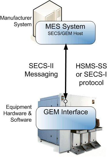
In a factory SECS/GEM implementation, there are two parties, the host, and equipment.  The equipment runs GEM interface software, which must implement and comply with the SEMI standards, on one of its computers.  The manufacturer (factory) runs GEM host software that establishes communication with the equipment's GEM interface.

The SECS Messaging Primer is a companion to the Introduction to the SECS/GEM standard white paper available on the Cimetrix SEMI Standards web page.  That white paper provides an overview of the SEMI SECS/GEM standard. 


Topics: Industry Highlights, SECS/GEM, Semiconductor Industry

Cimetrix Japan K.K. Established

Posted by Cimetrix on Dec 14, 2010 5:00:00 PM

by Dave Faulkner

Executive Vice President, Sales and Marketing

Cimetrix Japan K.K. was officially incorporated on November 25, 2010.  The purpose of this new company is to demonstrate commitment to the Japanese OEM market, have a dedicated staff to grow Cimetrix business in cooperation with our distribution partners, and to provide even stronger customer support.  The company's directors will be Bob Reback, Dave Faulkner, Jodi Juretich and Kerry Iwamoto. 

The company will be managed by Mr. Kerry Iwamoto as General Manager and Representative Director.   Mr. Iwamoto started his association with Cimetrix as a customer when he worked for Innotech designing semiconductor process equipment.  Recently, he has worked for Cimetrix distributors CIM, ONC and Rorze.  Mr. Iwamoto brings a strong background in the semiconductor industry and Cimetrix products along with close relationships with existing Cimetrix customers in Japan.

Watch for more news as we launch Cimetrix Japan.

Topics: Semiconductor Industry, Doing Business with Cimetrix, Global Services

Cimetrix at SEMICON Japan 2010

Posted by Cimetrix on Dec 14, 2010 11:35:00 AM

By Dave Faulkner

Executive VP, Sales and Marketing, Cimetrix

We had a strong showing at SEMICON Japan at the Makuhari Messe December 1 - 3.  Attendance was brisk, and Cimetrix products were on display at both the Meiden and the Rorze booths.  This event was a great opportunity for us, since we have just started Cimetrix Japan K.K. effective November 25, 2010.  The new Cimetrix company will provide both new market development and customer support for the Japan marketplace.

In the Meiden booth, Cimetrix EDA/Interface A products were on display.  In addition, Meiden highlighted the partnership between Meiden, DSD, and Cimetrix, which allows DSD and Meiden to offer complete EDA solutions using Cimetrix technology.  These solutions are available to both equipment suppliers and IC manufacturers, and Meiden listed the benefits and sample architectures for each group. 

 meiden_booth-resized-600-1

 Cimetrix CIMControlFramework (CCF) was on display at the Rorze booth running a complete 450mm vacuum platform.  Many visitors stopped to watch this powerful demonstration.  Cimetrix products were also highlighted, along with Rorze’s unique ability to deliver a complete hardware/software platform solution for equipment suppliers using Rorze and Cimetrix technology. 

 Rorze Booth resized 600

 One other highlight of the show was visiting the Axcelis booth where they highlighted their Integra plasma dry strip cleaning system that uses the Cimetrix CIMControlFrameworkaxcelis_booth_integra_tool_using_ccf-resized-600-2

We also learned at the show that a new top 20 OEM in Japan would adopt Cimetrix connectivity products.  It is great to see how companies are using our solutions to get to their products up and running in wafer fabs around the world.

Thanks to all those people who stopped by the booths.  Please let us know if you need more information about Cimetrix connectivity or tool control solutions.

Topics: Semiconductor Industry, EDA/Interface A, Events, Data Collection/Management, Cimetrix Products

Revisiting SECS/GEM: The Other Side of the Wire

Posted by Cimetrix on Dec 6, 2010 2:49:00 PM

by David Francis
Product Manager

Many years ago, I had the opportunity to work with some large semiconductor companies, including, Intel, Motorola, Lucent, and Siltronic.  I developed interface acceptance tests for equipment they purchased.  At that time, the SEMI SECS/GEM standards were still new and not widely adopted.  Many of the tool vendors had little or no previous experience writing SECS/GEM interfaces, and they were often uncertain about the details of the standards, along with worrying about how they could comply with them.  Chief among the vendors’ concerns was how they could meet their design schedules without loading down their engineering teams with this new requirement placed upon them. 

Over the intervening years I worked in the scheduling and dispatching area of automated semiconductor manufacturing, and in that time I lost track of the SECS/GEM standards and their adoption by the wafer fabs.

IBM Fishkill Photo resized 600


Recently I joined Cimetrix as Product Manager for the connectivity and tool automation products, and now I am back in the world of SECS/GEM standards.  A lot has changed since those early years, as fabs moved from 200mm to 300mm, and now considering 450mm wafer fabrication.  In addition, the geometries have shrunk from 1 micron down to 40nm and below.  However, I still see many of the same industry concerns as I did many years ago, even though there has been little change to the SECS/GEM standards.

The real change I see is the wide spread adoption of the SECS/GEM standard.  Previously, only a few leading edge companies requested SECS/GEM interfaces on their tools and were working feverishly to set up host-side equipment controls.  Today, SECS/GEM is well rooted in 300mm semiconductor manufacturing and tool vendors have very mature automation interfaces.

The move to 300mm processing created an ideal opportunity for the development and adoption of the GEM300 standards. Building new 300mm tools created an ideal environment for designing in the GEM300 standards right from the start.

More recently, new standards, like Interface A, have emerged from their R&D phase and are now going through the same refining process that SECS/GEM went through a decade ago.  These new standards will continue to support the industry’s efforts to create more efficient devices, at ever-decreasing geometries, with increased reliability and yield quality.

It is exciting to be working with these standards again and looking at them from the other end of the wire – the tool-side as opposed to my previous fab-side experience.  I look forward to writing more about how the tool vendors are adopting, and demonstrating compliance, to the new standards.

Topics: SECS/GEM, Semiconductor Industry, EDA/Interface A

SCW10 Follow Up

Posted by Cimetrix on Jul 19, 2010 4:48:00 PM

We've returned home from the show... tired, but excited about some of the great discussions and opportunities from the show! Although it was evident that SEMICON West is changing, it was also clear that the industry is rebounding and many new projects are getting underway.

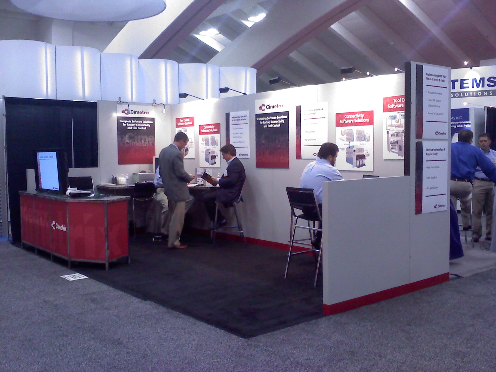
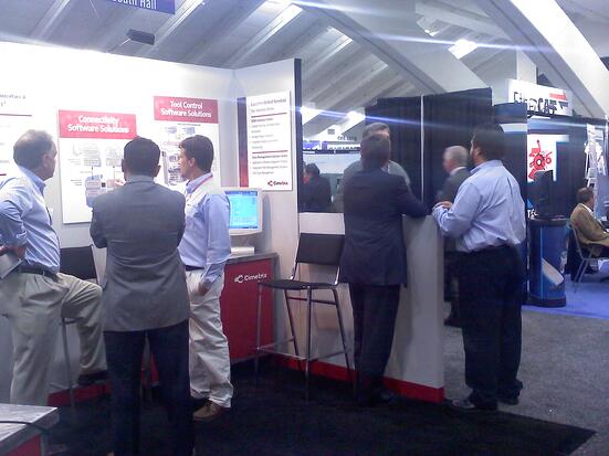
Here a couple of quick snap shots of our booth:

SEMICON West 2010 Booth

SEMICON West 2010 booth 2

We will be following up with visitors and customers this week. If you saw us at the show, thanks for stopping by and we look forward to continuing the conversation!


Topics: Semiconductor Industry, Events

SEMICON West 2010

Posted by Cimetrix on Jul 8, 2010 12:57:00 PM

describe the imageThe semiconductor industry's largest event of the year, SEMICON West, is right around the corner.  And with the market in recovery, we expect it to be a good turn out and a great show.

This year, Cimetrix has several exciting new developments to discuss at the show:

  • GEM Implementation - Faster & Better
    We've been at work developing a new solution that enables an even faster GEM implementation... while still improving the already high level of quality you've come to expect from Cimetrix. Designed to cover 90% of typical GEM interfaces, the new solution helps reduce time to market (and headaches) for our customers.
  • The Year for Interface A - Are you Ready?
    ISMI announced the new Freeze Version of the Interface A Standards on June 17. Also, with increased SEMI investment and fabs requiring implementation, this has quickly become a hot topic. Is your software able to support multiple versions of the Interface A standard at the same time? Are you set up to adopt the new version effectively and efficiently?

We would love the opportunity to discuss your unique needs and projects with you further at the show.

Not registered for the show?  Email us for a free pass.

We will be in the South Hall - Booth #2331.

See you at the show!

Topics: SECS/GEM, Semiconductor Industry, EDA/Interface A, Events

Fabs are like people

Posted by Cimetrix on May 27, 2010 6:00:00 AM

by Brent Forsgren,
Director of OEM Solutions

people like fabsFabs are like people, each one has it own personality traits. Fortunately, and arguably unfortunately, unlike people, most fabs have a handbook for their “personalities” in the form of specifications. I have found it interesting, that like people, fab “personalities” have common and unique features. Here are a few of examples:

  • There are some fabs that I would classify as the “Clean Freak.” Compliance to GEM and GEM 300 standards is important but more important to them is preventing cross contamination between FOUPs, and from wafer to wafer – “Who left this loadport door open? Don’t you know you can spread particles by doing that??”
  • Then there are other fabs that I would classify as the “Punctilious.” Again, compliance to the GEM and GEM300 standards is required but more important to them is knowing exactly when you are going to be done, when you are ready for more, are you done yet, how much longer are you going to be, are you done yet?
  • Then there are other fabs that are “Methodical-ious” (if I can make that a word). Everything must happen in a very specific order. 1) Don’t allow jobs to exist without material at the tool first; 2) Download the recipe before every job that is created; 3) Create the job now. 4) If the FOUP is removed before the job starts, refer to rule 1.
  • And let’s admit it, all fabs are “Control Freaks,” if they weren’t we wouldn’t be in business. They control when jobs are run, how jobs are run, and what a job does.

Hmmmm……that makes me wonder, if fabs are like people, does that make companies like Cimetrix psychiatrists?

Topics: Industry Highlights, Semiconductor Industry, Doing Business with Cimetrix

SEMI E148: Time Synchronization

Posted by Cimetrix on Mar 18, 2010 8:31:00 AM

by Doug Rust,
Director, Product Engineering & Customer Support

time synchronizationThe time shift for daylight savings this week is going to cause me some grief for some time. Most countries in Europe will not adjust until March 28. Many countries in Asia (India, Singapore, Taiwan, Malaysia and Japan for example) are not adjusting for daylight savings at all in 2010. Since our customers are all over the world, I’m going to have a tough time keeping in sync. It’s inevitable that I’ll miss some important event this month. So, I thought it would be very àpropos to submit a blog about Time Synchronization.

SEMI® standard E148 defines software standards for the equipment communication interface to enable the equipment control computers to automatically synchronize their clocks from a standard time base. Although this standard was just published a couple years ago, it is not new technology. Computer systems have been using internet technology to synchronize their clocks with a common time base for over 20 years now. The Network Time Protocol (NTP – a.k.a RFC1305) is the internet standard for time synchronization that is designed to enable any computer to synchronize with a reference clock (most commonly the atomic clock in Colorado) through various time servers available on the internet. SEMI E148 specifies the NTP standard as the mechanism for synchronizing the equipment control computer with the factory computer systems (as well as some other requirements).

This is becoming a critical capability as factories begin to adopt other information technology that enables them to collect thousands of precise data points from each run on each tool. Making effective use of this data requires that the time-base for data source ‘A’ is the same as the time base for other data sources so that the raw data can be assimilated and correlated to produce valuable manufacturing information. If there was some important “event” in manufacturing that we need to analyze the first thing we will do is to try to determine what else was happening at the time of that event. So the first question we ask is “when did that occur?” That’s where we can run into serious problems if there is no common time base.

Most modern operating systems have the NTP client software built-in. It’s possible to synchronize with reliable time servers on the internet and there are many affordable commercial time servers available. Even if users do not implement all of the E148 requirements, I suspect we are going to see more and more factory networks using NTP to synchronize the manufacturing equipment with factory hosts over the next year (if they haven’t already done it). For me, I guess I’m going to be out of sync at least until May 28.

Topics: Industry Highlights, Semiconductor Industry