Industry News, Trends and Technology, and Standards Updates

Summer 2020 North America ABFI Task Force Report

Posted by Brian Rubow: Director of Solutions Engineering on Aug 5, 2020 11:00:00 AM

Background

The SEMI North America Advanced Backend Factory Integration (ABFI) task force is part of the North America Information and Control Committee (I&CC or NA I&CC). Normally this task force meets every July in San Francisco as part of SEMICON West. However, this year the technical committee meetings are spread out over several weeks and do not coincide directly with the exhibition. Additionally, the I&CC did not meet at all because SEMI regulations do not currently allow TC Chapter (Committee) voting in virtual meetings. That will hopefully change later this year, but for now delays SEMI standards development.

Regardless of these challenges, the ABFI task force did meet on Monday July 13, 2020 and continues to develop SEMI standards. I am co-leader of the NA ABFI task force along with Dave Huntley of PDF Solutions. This blog is a summary of the current task force activities.

Wafer Maps

Ballot 6648 to update to the SEMI E142 (Specification for Substrate Mapping) specification has passed initial voting and is recommended to be accepted and published. This ballot significantly enhances the amount of traceability data that may be embedded within wafer maps.

Additional Wafer Map Activity

Because wafer maps will potentially be much larger with additional traceability data, they could be too large for the messages currently defined in the E142.2 standard. A new activity has been started to modify wafer map usage further and to allow Stream 21 messages to be used for wafer map transfer. The stream 21 message in the SECS-II standard can be used to transfer very large items through a GEM interface.

SEMI Standard Usage Matrix for Backend

The ABFI task force is also defining a matrix that specifies which standards beyond GEM (E30), SECS-II (E5), HSMS (E37) and Substrate Mapping (E142) should be used for backend automation, and under what conditions they should be used. This includes consideration of the full suite of GEM 300 standards and other standards that all GEM interfaces should consider, such as SEDD (E172) and SMN (E173).

Getting Involved

For those interested in participating, it is easy to join SEMI standards activities. Anyone can register at www.semi.org/standardsmembership.

All SEMI task force ballot activities are logged at http://downloads.semi.org/web/wstdsbal.nsf/TFOFandSNARFsbyCommittee?OpenView&Start=1&Count=1000&ExpandView

After joining the standards activities, anyone can get involved. The task forces post everything on the connected @ SEMI website https://connect.semi.org/home. The North America ABFI task force does not have a community.

To learn more about the standards, or to speak with a standards expert, click on the button below:

Ask an Expert

Topics: Industry Highlights, Semiconductor Industry, Standards

Cimetrix welcomes Thomas Simon as Director of Sales of Cimetrix Europe!

Posted by Cimetrix on Jul 30, 2020 8:00:00 AM

MicrosoftTeams-image (21)Cimetrix is pleased to announce and welcome Thomas Simon as its Director of Sales of Cimetrix Europe and Managing Director of Cimetrix GmbH. Thomas is based in Munich, Germany and will lead our growth in Europe. Thomas Simon will be responsible for ensuring the success of our growing customer base of leading semiconductor equipment manufacturers and smart manufacturing factories in Europe, providing strategic direction for Cimetrix Europe to have long-term success in the European market, overseeing local sales and account management and leading an expert team of Europe-based software engineers.

Thomas earned a Master of Science in Electronics and Semiconductor Technology and has 29 years of experience in the semiconductor, semiconductor backend, and electronics industries. He started his career as a field service engineer and then field service management working for companies such as Robert Bosch, SPTS (KLA), Centrotherm, UNAXIS (Evatec) and Suss MicroTec. Since 2011, Thomas has worked for Ulvac as Director of Sales and Business Development.

“Cimetrix has been serving European customers in the semiconductor and electronics markets for over 20 years. We have worked hard to gain a reputation for high quality products that are backed by responsive and exceptional technical support. Today, this provides us with a solid foundation of many longtime customers willing to serve as enthusiastic references. We also see strong and growing demand for Industrie 4.0 and Smart Manufacturing solutions. Accordingly, Cimetrix made the strategic decision to hire an experienced professional to lead Cimetrix’s business in Europe. We are very fortunate to have found Thomas Simon, as his vast experience in the semiconductor and electronics industries is a great fit with Cimetrix. We look forward to growing the Cimetrix team in Europe to provide even higher levels of support to our European customers.” 

-Bob Reback, President and CEO

Cimetrix has been building international teams throughout the world to provide our clients with technical experts who work in their local time zones, speak their native languages, and understand their unique cultures. In all of the major regions for semiconductor and electronics manufacturing, we now have an experienced executive who serves as that region’s Managing Director and is able to help our customers be successful and receive the highest levels of technical support.

To contact Thomas, please click the button below. Welcome Thomas!

Contact Us


Topics: Industry Highlights, Customer Support, Doing Business with Cimetrix, Meet Our Team

Cimetrix 2020 Annual Shareholder Meeting is Postponed

Posted by Bob Reback: Chairman, President, and Chief Executive Officer on Jul 29, 2020 10:23:25 AM

To our Cimetrix shareholders,

One of the highlights of the year is the annual Cimetrix shareholder meeting, which is typically held in August at the Company’s headquarters office in Salt Lake City. We always enjoy the gathering of shareholders and reporting on the Company’s progress. The 2020 annual meeting has been on the calendar for Friday, August 14, and our hope was things would be back to normal by that time. Unfortunately, there has been a recent surge in COVID-19 cases in Utah, and we believe it would not be prudent to host the annual shareholder meeting at this time. Our number one concern is the safety of our shareholders and employees. Consequently, the Cimetrix 2020 annual meeting is officially postponed until further notice.

While the Company’s business has been impacted by COVID-19, we have transitioned to enable all employees to work from home. Demand within the semiconductor and electronics industries remains strong for our products, and we believe we are on track to meet our overall 2020 plans. Cimetrix has retained all of its valuable employees and is in the process of recruiting additional team members.

Once we set a new date for the annual shareholder meeting, we will report it on our website and send out another notice to shareholders. We thank our shareholders for their concerns and support.

Sincerely,

Bob Reback
President and Chief Executive Officer

For future updates and investor information, please visit our Investor Relations Page.

Topics: Industry Highlights, Doing Business with Cimetrix

Summer 2020 North America GEM 300 Task Force Report

Posted by Brian Rubow: Director of Solutions Engineering on Jul 22, 2020 10:45:00 AM

Background

The SEMI North America GEM 300 task force is part of the North America Information and Control Committee (I&CC or NA I&CC). Normally this task force meets in San Francisco as part of SEMICON West. However, this year the technical committee meetings are spread over several weeks and don’t coincide directly with SEMICON West. Additionally, the I&CC did not meet at all because SEMI regulations do not currently allow TC Chapter (Committee) voting in virtual meetings. That will hopefully change later this year, but for now inhibits the pace of SEMI standards development.

However, the GEM 300 task force did meet on Monday July 13, 2020, and continues to develop SEMI standards. I am co-leader of the NA GEM 300 task force, along with Chris Maloney from Intel. This blog is a summary of the current task force activities.

Pre-Meeting Summary

The table below contains a summary of the worldwide activities related to the GEM 300 task force as of the start of this summer’s meeting. There are corresponding task forces in the Japan and South Korea regions which are also active.

Region

Ballot

Standard(s)

Status

Topic

South Korea

5832

New

Cycle 5, 2020

Generic Counter

North America

6348

E30

Published

SEMI style/regulation conformance

North America

6572

E30

Development

Add Stream 21, Cleanup Process Program Management.

North America

6552

E5

Cycle 5, 2020

Data collection setup, terminology

North America

6598

E37, E37.1

Cycle 5, 2020

Standardize TCP/IP port numbers

North America

6597

E173

Adjudication Pending

Minor updates, clarification

Awaiting I&CC adjudication from cycle 2, 2020 voting (no negatives) and the task force recommendation from Spring 2020.

North America

6647

E116

Development

Recommendations from the ABFI task force


Current Ballot Activity

Two ballots were adjudicated during the most recent GEM 300 task force meeting. For those of you new to the standards development process, the term “adjudication” means that we review the results of the voting and recommend handling of all negative votes and comments received. The recommendations by the task force are then presented to and finalized at the committee level. Since the North America I&CC did not meet, the failed and super-clean ballots are being transferred to other regions (probably Taiwan) for further processing. Passed ballots with any negatives or comments are put on hold until NA I&CC meets so that the merits of the comments and overridden negatives can be evaluated.

6552A E5

This ballot modifies the E5 SECS-II standard. The ballot included three line-items, each of which is voted on separately

  1. This is the most exciting activity in this ballot because it will give GEM host software much better tools for managing and testing GEM data collection. The first line item proposed adding several new messages to the E5 standard including a message to:
    1. Query the list of defined report identifiers
    2. Query report definitions
    3. Query a list of event report links
    4. Query the list of enabled events (this could already be done using Status Variable EventsEnabled)
    5. Query the list of streams and functions configured for spooling
    6. Query the list of defined trace identifiers
    7. Query trace definitions
  1.  
  2. Establish proper definitions for status variables, data variables and equipment constants. Additionally, deprecate the usage of the data item “DVNAME” which has generated confusion for years since it means a data variable identifier and not a data variable name.
  3. Clarify the usage of message S7F17/F18. This message allows deletion of one or more recipes, but only returns a single acknowledgement code. The new clarification defines what to expect when an error is returned.

Each of the line items had at least one comment or negative; therefore, none was super-clean. The GEM 300 task force decided to pass line items 1 and 3, but fail line item 2.

6598A E37

The primary purpose of this ballot is to clarify some confusing text related to the T8 timer. Additionally, there are other improvements related to recommended settings. The GEM 300 task force decided to fail this ballot.

New Ballot Activity

Here is a summary of the next set of ballots to expect from the NA GEM 300 task force planned to be presented for Cycle 7 voting later this year.

Ballot

Specification

Description

6552B

E5

A rework of ballot 6552A line item #2, which is described above.

6598B

E37

A rework of ballot 6598A described above.

6647

E116

Recommendations from the ABFI task force to allow the GEM host to declare scheduled/unscheduled down time and for the equipment to declare an Engineering mode. This will allow E116 to map better to E10.

6572

E30

A major change to the GEM standard to officially allow usage of Stream 21 for large unformatted recipes and E172 SEDD files, deprecation of some little used recipe alternatives like E42, implementation of the new E5 messages from ballot 6552A line item #1, and several other enhancements.

Note that the ballot number will be changing due to a late scope change.

?

E148

Upgrade NTP from version 3 to version 4.


Getting Involved

For those interested in participating, it is easy to join SEMI standards activities. Anyone can register at www.semi.org/standardsmembership.

All SEMI task force ballot activities are logged at http://downloads.semi.org/web/wstdsbal.nsf/TFOFandSNARFsbyCommittee?OpenView&Start=1&Count=1000&ExpandView

After joining the standards activities, anyone can get involved. The task forces post everything on the connected @ SEMI website https://connect.semi.org/home. The North America GEM 300 task force community is called “GEM 300 Task Force - North America”.

To find out more about SEMI Standards, GEM300, or to talk to standards expert, click the button below. 

Ask an Expert

Topics: Industry Highlights, SECS/GEM, Semiconductor Industry, GEM300

Semiconductor Backend Processes: Additional SEMI Standards Related to GEM

Posted by Brian Rubow: Director of Solutions Engineering on Jul 9, 2020 11:30:00 AM

Background

In a few previous blogs I shared how the relatively new SEMI Advanced Backend Factory Integration (ABFI) task force in North America has already decided to promote the adoption of the GEM standard and selective adoption of the GEM300 equipment communication standards. In this blog I will summarize the task force’s plans to consider adoption of additional SEMI information and control standards that are complementary to GEM and GEM300.

Additional SEMI Standards for the Backend Consideration

Many of the standards listed below were developed a few years after GEM300 but are now considered to be part of the modern GEM300 set.

SEMI Designation

Standard Name

E84

Specification for Enhanced Carrier Handoff Parallel I/O Interface

E116

Specification for Equipment Performance Tracking

E116.1

Specification for SECS-II Protocol for Equipment Performance Tracking (EPT)

E142

Specification for Substrate Mapping

E142.1

Specification for XML Schema for Substrate Mapping

E142.2

Specification for SECS-II Protocol for Substrate Mapping

E148

Specification for Time Synchronization and Definition of the TS-Clock Object

E157

Specification for Module Process Tracking

E172

Specification for SECS Equipment Data Dictionary (SEDD)

E173

Specification for XML SECS-II Message Notation (SMN)


E84 Carrier Handoff

E84 Carrier Handoff is the only standard in this list that not a GEM standard because it deals with a separate parallel I/O interface. This interface is completely independent of GEM, although it is coordinated with E87 Carrier Management when both are supported. However, since E84 Carrier Handoff is often included in the GEM300 discussions and requirements, it is worth discussing here because it is a standard that the Backend industry should selectively adopt.

GEM-Backend-2-1

The E84 standard defines the handshake signals for use in a parallel I/O (PIO) interface to automate carrier delivery and carrier removal. The automated material handling system (AMHS) might use either an automated guided vehicle (AGV) or overhead transport (OHT) system, yet either way, the material is delivered in a carrier. E84 is widely used and accepted in every semiconductor wafer fab (front end) and an obvious choice for backend manufacturing when delivering carriers.

E116 Specification for Equipment Performance Tracking

E116 Equipment Performance Tracking was discussed in an earlier blog since there are plans to update this specification to better support backend operations. E116 is applicable to any manufacturing equipment in any industry because it is largely based on SEMI E10 principles which define generic terms for measuring any equipment’s reliability, availability and maintainability. As a bonus, each major component in the equipment can also be modelled to track its productivity.

E142 Specification for Substrate Mapping

E142 Substrate Mapping and its subordinate standards (E142.1 XML Schema for Substrate Mapping and E142.2 SECS-II Protocol for Substrate Mapping) define generic substrate maps and how to transfer them to and from an equipment through a GEM interface. Substrate maps are two dimensional arrays of data that correspond to a physical substrate—which may be a wafer, strip or tray. The map defines the dimensions of the substrate, significant locations on the substrate, and can include data about the locations (such as a numbering scheme for unambiguously identifying specific locations). For example, E142 can be used to tag “known good” devices on a substrate.

Some equipment types require a substrate map before processing can proceed. Some equipment can generate substrate maps. And some equipment both require a substrate map before processing and generate an updated substrate map after processing is completed. In E142, the substrate map is expressed in an XML file that conforms with the E142 XML schema. A lot of backend equipment need substrate maps for normal operation, so E142 is an obvious choice. Note that E142 is currently undergoing some interesting improvements via the ABFI task force to store additional data needed to address enhanced traceability requirements.

Substrate mapping is an excellent demonstration of horizontal communication implemented using GEM. Horizontal communication is when data is shared directly from one equipment to another equipment. Traditionally, horizontal communication in GEM is implemented indirectly; one equipment passes data to the host and then the host passes that data on to the equipment that needs it. In this sense, the GEM host acts as a type of broker between units of equipment.

There are significant advantages in using this indirect style of horizontal communication. For example, Equipment A might inspect a substrate, generate a substrate map and send it to the host. Equipment B might later request the substrate map from the host.

GEM-backend-2-2The benefit of using a GEM host between the equipment to realize this use case is that both Equipment A and Equipment B are only required to implement GEM—which they should be doing anyway. The equipment are not required to support additional protocols and/or custom message sequences, or to be tested against specific equipment interfaces. If each equipment follows the GEM standard, they can all be integrated into the factory system and share data through the GEM host.

E148 Specification for Time Synchronization and Definition of the TS-Clock Object

A lot of data collected in the factory is only useful when properly timestamped. Moreover, timestamps can only be compared among data from multiple sources when those timestamps are synchronized. This is where SEMI E148 enters the picture.

The E148 Time Synchronization specification requires equipment to support the industry standard Network Time Protocol (NTP) and share information about its implementation. And NTP software synchronizes computer clocks.

Because the backend industry segment is trending towards more and more data collection, it is critical to have proper timestamping for that data, and therefore time synchronization for its sources. A full E148 implementation may not be required, but certainly the equipment should support NTP as described in E148. If an equipment control systems is composed of multiple computers, E148 states that they should all be synchronized with a single computer designated as the master, which is a good idea if the other computers are generating data with timestamps.

E157 Specification for Module Process Tracking

E157 Module Process Tracking does not apply to all backend equipment. To use E157 Module Process Tracking, there must be at least one process module (aka a process chamber) which processes one substrate or a batch of material at a time. If multiple substrates are processed at a time but each having different start and stop times, then this specification cannot be applied.

E157 Module Process Tracking defines a very simple processing state model which is implemented independently for each process chamber.

GEM-backend-2-3The state model reports when the process chamber is either idle (Not Executing) or processing a recipe (Executing). And when processing a recipe, each time an individual step in the recipe starts, completes, or fails, this is reported. It is up to the implementer to decide what constitutes a recipe step. In my experience, most equipment that could adopt E157 have already implemented something very similar using a set of GEM events. However, rather than implementing something custom, it is better for end users and equipment manufacturers alike if the implementations are standardized.

E157 is a prime example of an exceptionally simple and well-written standard built on top of GEM technology that is easy to implement and provides a lot of end user value. Hopefully the ABFI task force can develop something based on E157 principles that is well suited for backend equipment that cannot accommodate the full scope of the current standard.

E172 Specification for SECS Equipment Data Dictionary (SEDD)

Go back in time (not that far, actually), and “GEM documentation” meant a stack of printed documentation on paper that was expected to be delivered with the equipment. Today “GEM documentation” means an MS Word document, PDF file, Excel spreadsheet, or some other electronic representation of the same information. Nearly any digital format is acceptable.

Nevertheless, E172 SECS Equipment Data Dictionary is the future of GEM documentation. The GEM documentation is provided in a standardized electronic XML format called an SEDD file. E172 defines a standard XML schema. The initial version of this schema included only basic information about a GEM interface. This was expanded in a later version to include several more details. Soon, I hope to report that the E30 GEM standard has been modified to officially include SEDD files as one form of documentation. Additionally, this should include enhancing the GEM standard to allow an SEDD file to be transferred directly through the GEM interface. This will significantly improve GEM’s plug-and-play capability by enabling factory host software to consume an SEDD file and automatically configure the GEM host software to support an equipment’s specific implementation of GEM and GEM messages.

As the backend industry segment is increasingly implementing GEM in its factories, I expect SEDD files to be required from all backend equipment manufacturers.

E173 Specification for XML SECS-II Message Notation (SMN)

In order to diagnose problems in a GEM interface, it is essential to have logging for the GEM messages transferred between the host and equipment. Typically, both the GEM host and equipment’s GEM interface will provide logging functionality. In the past, a notation called SML (SECS Message Language) was used for logging GEM messages. Unfortunately, SML was never standardized or even sufficiently well defined. As result, there are many different variations of SML throughout the world. While SML notation itself is relatively easy to generate with software, the breadth of implementation variations makes it difficult to automatically parse and use.

Fortunately, the SEMI North America GEM300 task force created E173 XML SECS-II Message Notation (SMN) to solve this problem. SMN defines an XML schema that anyone can use to document and log GEM SECS-II messages. The schema is feature rich allowing for both minimum and elaborate XML decoration. As an example of its usefulness and flexibility, the E172 SEDD schema references the SMN schema file. Because SMN is based on XML, it is both very easy for software to generate and consume. There are numerous software tools and libraries available in virtually every software programming language for working with XML. Using SMN with GEM allows GEM to continue to send and receive messages in an efficient binary format, yet still enjoy the benefits of using a decorated, human-readable text notation for diagnosing issues.

I expect the ABFI task force to recommend that the backend industry segment adopt SMN in all equipment GEM interfaces.

Conclusion

As backend factories adopt GEM, we expect that they will also want to use the latest technologies with it, including SMN, SEDD, Module Process Tracking and Equipment Performance Tracking. Watch for more details and updates from the SEMI Advanced Backend Factory Integration task force as its work progresses—and feel free to join this initiative if you want to help steer and accelerate this activity!

To download the GEM300 White Paper, click the button below.

GEM300


Topics: Industry Highlights, SECS/GEM, Doing Business with Cimetrix, GEM300

Semiconductor Back End Processes: Selective GEM300 Adoption

Posted by Brian Rubow: Director of Solutions Engineering on Jun 24, 2020 11:15:00 AM

GEM and GEM300 Adoption

In a previous blog I shared how the relatively new SEMI task force in North America called “Advanced Back End Factory Integration” (ABFI) has already decided to promote the adoption of the GEM standard. In this blog I will explain how the task force is also planning to selectively adopt what is often called the GEM300 set of standards. I say “planning” because this is a work in progress and subject to the standardization process in which we strive for consensus among the participants. However, one can argue that this plan should not be particularly controversial since the GEM300 standards have already been adopted by several major manufacturers of semiconductor back end equipment.

What are the GEM300 Standards?

There is no official “GEM300” definition, but at a minimum, all the experts agree that the GEM300 set of SEMI standards includes the following:

SEMI Designation

Standard Name

E5

Specification for SEMI Equipment Communications Standard 2 Message Content (SECS-II)

E30

Specification for the Generic Model for Communications and Control of Manufacturing Equipment (GEM)

E37

Specification for High-Speed SECS Message Services (HSMS) Generic Services

E37.1

Specification for High-Speed SECS Message Services Single Selected-Session Mode (HSMS-SS)

E39

Object Services Standard: Concepts, Behavior, and Services

E39.1

SECS-II Protocol for Object Services Standard (OSS)

E40

Standard for Processing Management

E40.1

Specification for SECS-II Support for Processing Management

E87

Specification for Carrier Management (CMS)

E87.1

Specification for SECS-II Protocol for Carrier Management (CMS)

E90

Specification for Substrate Tracking

E90.1

Specification for SECS-II Protocol for Substrate Tracking

E94

Specification for Control Job Management

E94.1

Specification for SECS-II Protocol for Control Job Management (CJM)


Seen together like this in a table, it seems like a lot to study and learn. And it is daunting. However, it is important to remember that most of the primary standards (like E87 and E90) also have a subordinate standard (like E87.1 and E90.1) that defines how to implement the standard using SECS-II. Although this nearly doubles the length of the list, these “.1” standards are really just extensions of the primary standard, and are all relatively short specifications. Each of these core GEM300 standards defines specifically how to use and augment the GEM standard to implement specific factory automation requirements and production operational scenarios. Basically, they work together like this:

GEM-for-Backend-2.1

SEMI E37 (High-Speed SECS Messaging Services), E5 (SECS-II) and E30 (GEM) are the core standards for any modern GEM implementation—regardless of the GEM300 additions—so of course they apply. Each of the additional GEM300 standards builds on top of E30 and E5 to define general features for data collection, alarm handling, collection event reporting and the messaging library. For example, E87 (Carrier Management) deals with the load port services, carrier delivery, and carrier removal. E90 (Substrate Tracking) reports all substrate movement from the carrier to the process chamber and any intermediate movement. E40 (Processing Management) and E94 (Control Job Management) determine which substrates to process, which recipes to use and the substrate destinations. Finally, E39 (Object Services) defines general object handling for all of the standards.

Even though the diagram shows silicon wafers—since semiconductor front end factories use this set of GEM300 standards nearly universally—their applicability goes well beyond 300mm silicon wafer processing. However, if an equipment does not deal with the substrates (material) or substrate delivery directly, then it is best just implementing GEM rather than GEM300.

How can these SEMI standards be applied to other equipment?

E87 Carrier Management

Certainly, any equipment dealing with a FOUP (front-opening universal pod) that holds silicon wafers can adopt E87 Carrier Management to manage the load ports and carrier validation. But E87 Carrier Management is written in a manner flexible enough that equipment handling many other types of material can adopt it. Here are the criteria:

    1. The material arrives in a container of some sort.

      The shape of the container, the number of slots in the container and the orientation of the slots do not matter. The container can be a rectangular tray with pockets. It can also be round with pockets. E87 Carrier Management refers to these containers as carriers.
    2. The material slots in the container can be ordered.

      In a FOUP, the material is in a horizontally stacked orientation. However, the principles of E87 Carrier Management can also apply to other material orientations. Whatever the container type, there needs to be clearly defined slot numbering. E87 Carrier Management only defines the order for a stacked container; therefore, other container styles need standardization.

With these two criteria, E87 Carrier Management can be applied to add value to the equipment by supporting an increased level of factory automation.

What features determine whether E87 Carrier Management can be adopted?

    1. Carrier (Container) ID

      If there is a carrier ID of some sort, it is of course very useful for implementing carrier ID verification. The carrier ID can be a barcode or any other type of identifier. But even if there is no carrier ID (even a barcode would suffice), then while under remote control the host can assign an ID to the carrier. Alternatively, while under local control the equipment software can generate a unique carrier ID.

    2. Carrier (Container) ID Reader

      E87 Carrier Management anticipated that a unit of equipment might not have a carrier ID reader. It also anticipated that a carrier ID reader might be out of service or defective, and therefore should be ignored. Not having a carrier ID reader means that you will not have the benefit of verifying that the correct container has arrived.

    3. Number of Slots in the Container

      A standard FOUP for silicon wafers has 25 slots. But the number of slots in a container is not limited or restricted.

When can’t E87 Carrier Management be applied?

For E87 Carrier Management to be applied, the material needs to arrive and/or depart in some sort of container. If material arrives and departs continuously without any container, such as on a conveyor, then there is no container or load port for E87 Carrier Management to manage. Of course, GEM can still be applied without E87 and the other GEM300 standards, although E90 Substrate Tracking might still be useful.

What are the benefits of using E87 Carrier Management?

E87 Carrier Management provides quite a few benefits to any equipment that can adopt it.

  • Confirmation that the correct container arrived at the equipment
  • Confirmation that the container has the expected material in its various locations
  • Reporting current load port states (e.g., occupied, ready for unloading, ready for loading)
  • Placing a load port in and out of service, such as for maintenance and repair
  • Notifying the equipment when a container will be arriving
  • Managing container storage
  • Reporting when the material from a container is nearly completed processing
  • Load port identification
  • Assigning substrate IDs

E90 Substrate Tracking

The “substrate” term is not restricted to silicon wafers, but rather applies to any type of product material. This generalization of the substrate term means that E90 Substrate Tracking can be applied to many different types of equipment.

Normally substrate tracking is considered in terms of fixed substrate locations, such as a slot in a container, a specific location in a pre-aligner, the end effector of a robot arm, or a specific process chamber. However, just a like a robot for handling silicon wafers can have multiple arms for handling multiple substrates, a conveyor can be similarly modeled to have multiple substrate locations. For example, if a conveyor can hold 50 small substrates at a time, then it could be modeled with 50 substrate locations for high-precision material tracking. Doing so allows E90 to be used to track substrates even while on a conveyor. The time each substrate is placed on a conveyor can be used to deduce the order of the material on the conveyor.

E90 Substrate Tracking also provides for substrate ID verification. This is only possible when the substrates have an identification code that can be read, such as a barcode or 2D data matrix, and when the equipment has the hardware capable of reading the identification code. When both are present, substrate ID verification can allow the factory to confirm each substrate before processing, and thereby reduce scrap.

When an equipment transports and processes multiple units of material internally using any type of container, it is called batch processing. E90 Substrate Tracking also supports this method by identifying batch locations and by providing data collection features specific to batch movement.

When can’t E90 Substrate Tracking be applied?

In order to use E90 Substrate Tracking, the equipment must have at least two substrate locations and work with some type of substrate. Without these there is no benefit in implementing E90 Substrate Tracking.

What are the benefits of using E90 Substrate Tracking?

E90 Substrate Tracking provides many benefits to any equipment that handles material.
  • Providing history of substrate movement, including timestamps for each location change
  • Substrate identification
  • Substrate location identification
  • Factory substrate verification, including the automated rejection of invalid substrates
  • Providing processing status for each substrate
  • Implementing virtual substrate tracking for lost substrates

E40 Processing Management

E40 Processing Management creates a list of materials to process and the name of the recipe to use. When using silicon wafer substrates, this list is either in the form of a carrier ID and a set of slot numbers, or a list of substrate IDs.

When can’t E40 Processing Management be applied?

If an equipment processes material continuously without having a discrete set of material that is known and identified ahead of time, you cannot apply E40 Processing Management. E40 Processing Management assumes that you have a specific set of material to process. If each substrate is simply processed as it arrives, then you are better off just using GEM’s PP-SELECT remote command to choose the correct recipe.

What are the benefits of using E40 Processing Management?

E40 Processing Management provides multiple benefits when it can be applied to an equipment:

  • Easily configure the equipment to process a specific set of material with a specific recipe. For example, 20 substrates can all be processed with the same recipe, or each with a different recipe.
  • Allows the equipment to support process tuning in which specific default settings in a selected recipe can be overwritten with new values. This is far easier than creating a proliferation of nearly identical recipes.

E94 Control Job Management

E40 Processing Management can be used in a standalone fashion but is usually implemented in conjunction with E94 Control Job Management. I recommend implementing both. Even if you don’t need all the extra features of Control Job Management, it adds very little overhead and is easy to use.

When can’t E94 Control Job Management be applied?

E94 Control Job Management cannot be used without E40 Processing Management, because its primary function is to manage the E40 process jobs. Therefore, its applicability is subject to the same criteria as E40 Processing Management.

What are the benefits of using E94 Control Job Management?

E94 Control Job Management has some features that benefit some equipment:

  • Allows material to arrive in one container and depart in another. This is beneficial when the source container needs to be kept uncontaminated by the effects of a process.
  • Allows material to be sorted based on some criteria. This is beneficial when sorting takes place based on inspection and/or other conditions, and the material is subsequently routed to different destination containers based on the sorting.
  • Manages a set of process jobs. For example, one can abort, pause or resume all process jobs.

How does all of this apply to the back end industry segment?

Factories must decide if they want the benefits of GEM300. Although E90 Substrate Tracking can be applied to most equipment, E87 Carrier Management, E40 Processing Management and E94 Control Job Management are only applicable to the equipment that deliver and/or remove material in containers. The features of each standard may not seem remarkable in and of themselves, but it is important to remember that these features have been implemented in a standardized way that many equipment manufacturers and their factory customers around the world have all agreed to follow—and that is truly remarkable.

One of the primary benefits of the GEM300 standards is the factory’s ability to move material to the equipment and process it in any order. The term “process” is used very loosely with the understanding that in addition to material transformation, inspection, metrology, sorting, testing, packaging, and other manufacturing activities are all types of processing. The material can be moved from any equipment to any equipment. This flexibility is a key to the success of modern integrated circuit manufacturing. It allows for the fabrication of many products without moving equipment or setting up conveyors. It allows process steps to be added or removed at any time. It enables the optimum use of inspection and metrology equipment since the same equipment can be used before and after any process step. The GEM300 standards directly support this flexibility.

The SEMI Advanced Back End Factory Integration task force plans to standardize the criteria for determining which standards apply based on an equipment’s functionality. What I’ve explained in this posting is just the starting point for this work—there is much more to be done. We welcome more participants on the task force to ensure the standardization is done accurately and efficiently.

Contact Us

Topics: Industry Highlights, SECS/GEM, Doing Business with Cimetrix, GEM300

How we helped a customer deliver a GEM-compliant equipment using CCF

Posted by Rich Kingsford; Project Manager, CCF Services on Jun 4, 2020 2:30:00 PM

Welcome to the first posting in the Cimetrix CIMControlFramework (CCF) Services blog series! While Cimetrix has been providing professional services for many years, in order to better serve the growing demand from many new equipment maker customers worldwide that have purchased our CCF product, Cimetrix earlier this year formed a new CCF Services group, reporting directly to the CEO. Being a senior developer at Cimetrix for the past 15 years in a variety of positions, I was delighted when asked to lead this group. We have an outstanding team of software engineers highly experienced in factory automation, equipment control software and SEMI standards. We are dedicated to ensuring our customers’ success by providing training, consulting, and developing custom solutions for our CCF customers. We love learning about the myriad ways that companies can integrate CCF with their equipment to meet the material handling and factory automation requirements of their factory customers. Our goal for these articles is to share some of the lessons learned and other implementation insights to help you efficiently build manufacturing equipment that is sophisticated, robust, and productive. To this end, our first posting will deal with one of the most common requests we get – enjoy!

- Forward by Brent Forsgren, Director of CCF Services

How we helped a customer deliver a GEM-compliant equipment using CCF

The Goal

One of our recent customers wanted to build a new type of LED manufacturing equipment that could be controlled by a Factory Host using the standard GEM Remote Commands: PP_SELECT (Process Program Select), START, STOP, ABORT, PAUSE and RESUME. The equipment could be delivered in a variety of physical configurations, including 1-to-multiple source cassettes for product material, and 1-to-multiple process modules. It also had multiple destination cassettes to be filled according to the post-process analysis results. The initial instance of the equipment had 4 loadports (LPs) and four process modules (PMs).

The functional requirements were clear – that was the good news. Now for the rest of the story… the project schedule and budget constraints were closing in, so we needed to work quickly and efficiently with the customer to get it done. Sound familiar?

The Approach

The Cimetrix CCF Services team always works closely with the software team of the equipment manufacturer. In this case, we started with one week of mutual discovery and in-depth hands-on training. Team members were fully engaged and picked up the CCF capabilities very quickly. This included even some of the more advanced features, such as developing a scheduler that would control the components of the customer’s application. We regularly fine tune training modules to 1) introduce CCF concepts, 2) expose common challenges and potential approaches, and 3) provide realistic implementation practice exercises. As anticipated, the customer was able to use the results of the training exercises in the actual equipment control solution. We also kicked off the project with our work-breakdown exercise to more deeply explore the unique requirements for their specific equipment type.

After an intense first week, everyone on the project team concluded that CCF would in fact be a strong match for their needs. CCF features direct integration with our CIMConnect, CIM300, and CIMPortal connectivity products to provide full GEM, GEM300 and EDA compliance. Because the Cimetrix connectivity products are deployed in every semiconductor 300mm factory in the world, our customers can be assured that they will meet their customer’s factory automation requirements. In this application, the end customer’s LED factory only required GEM.

To address requirements that may go beyond the basic GEM standards, CCF also provides support for custom remote commands, data publication, and alarm management. Finally, CCF supports integrating custom hardware devices using CCF’s base Equipment Classes.

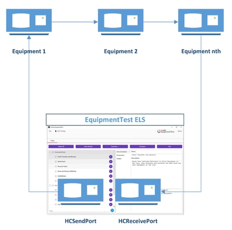
To prove all was working, we chose the Cimetrix EquipmentTest product to develop and execute a set of unit tests that emulate communications with the factory software using GEM messages. This was not intended to be a comprehensive set, but rather just enough to show the equipment passed round-trip system testing. In this context, round trip means showing that the equipment can move material from the incoming cassette to the aligner to the process module and back into the cassette. EquipmentTest also supports editing message settings and parameters on the fly to experiment with different configurations of a round-trip test.

The Challenge: “The Host is unavailable, but we need to validate that the equipment is both GEM compliant and accomplishes the communication flows the end user requires.”

We get this challenge a lot… Our customers almost always develop the host interface and the embedded control software in parallel and integrate them later in the project. This makes sense at one level, but it does introduce a “chicken and egg” problem for testing this kind of GEM interface. In particular, how can our customer provide evidence that the solution will work with the factory host without testing with the actual host system? Our answer: apply our EquipmentTest custom plugin capability to simulate the end user’s host so we can validate all necessary communication between host and equipment.

Our protocol validation product, EquipmentTest, makes it possible to simulate communications between an equipment control implementation and the host. And although it is impractical to implement scenarios for every possible interaction, we can create enough representative scenarios to be confident the “happy path” (i.e., no errors) will work and that the interface will handle a large handful of “sad path” cases as well.

CCF-Services-Image1

Outcome

We passed all the tests! “Let’s go get some tacos.”

Specifically, we validated that the communications interface supported…

  • Standard GEM Remote Commands
  • Custom Remote Commands
  • Material tracking
  • Data publication

In closing, we must emphasize that our customer should take most of the credit here. Nevertheless, we enjoyed observing, consulting, and testing the equipment. It is always gratifying to see the CCF solution fit so seamlessly into the hardware, execute its commands with optimal timing, and not break anything in the process! Truly a successful, joint team effort.

If the situation above resonates with your current challenges and past experiences, give us a call. We look forward to working with your software engineering team to speed your time-to-market and deliver a high-quality solution quickly, allowing your team members to focus on developing value-added functionality for your customers.

Topics: Industry Highlights, Equipment Control-Software Products, Doing Business with Cimetrix, GEM300

Semiconductor Back End Processes: Adopting GEM Judiciously

Posted by Brian Rubow: Director of Solutions Engineering on May 14, 2020 10:20:17 AM

Equipment Communication Leadership in Wafer Fabrication

For many years the semiconductor industry’s wafer fabrication facilities, where semiconductor devices are manufactured on [principally] silicon substrates, have universally embraced and mandated the GEM standard on nearly 100% of the production equipment. This includes the complete spectrum of front end of line (FEOL – device formation) and back end of line (BEOL – device interconnect) processes and supporting equipment. Most equipment also implement an additional set of SEMI standards, often called the “GEM 300” communication standards because their creation and adoption coincided with the first 300mm wafer manufacturing. Interestingly, there are no features in these standards specific to a particular wafer size.shutterstock_405869995_backend

Together, the GEM and GEM 300 standards have enabled the industry to process substrates in fully automated factories like Micron demonstrates in this video and GLOBALFOUNDRIES demonstrates in this video.

Specifically, the GEM 300 standards are used to manage the following crucial steps in the overall fabrication process:

  • automated carrier delivery and removal at the equipment
  • load port tracking and configuration
  • carrier ID and carrier content (slot map) verification
  • job execution where a recipe is assigned to specific material
  • remote control to start jobs and respond to crisis situations (e.g., pause, stop or abort processing)
  • material destination assignment after processing
  • precise material location tracking and status monitoring within the equipment
  • processing steps status reporting
  • overall equipment effectiveness (OEE) monitoring

Additionally, the GEM standard enables

  • the collection of unique equipment data to feed numerous data analysis applications such as statistical process control
  • equipment-specific remote control
  • alarm reporting for fault detection
  • interaction with an equipment operator/technician via on-screen text
  • preservation of valuable data during a communication failure

Semiconductor Back End Process Industry Follows the Lead

After wafer processing is completed, the wafers are shipped to a semiconductor back end manufacturing facility for packaging, assembly, and test. Historically this industry segment has used GEM and GEM 300 sporadically but not universally. This is now changing.

In North America, SEMI created a new task force called “Advanced Back end Factory Integration” (ABFI) to organize and facilitate this industry segment’s implementation of more robust automation capabilities. To this end, the task force is charged with defining GEM and GEM 300 support in back end equipment, including processes such as bumping, wafer test, singulation, die attach, wire bonding, packaging, marking, final test and final assembly. As its first priority, the task force has focused on updating the SEMI E142 standard (Substrate Mapping) to enhance wafer maps to report additional data necessary for single device traceability. Soon the task force will shift its focus to define GEM and GEM 300 back end use cases and adoption more clearly.

Why GEM?

GEM was selected for several reasons.

  • A lot of the equipment in the industry already have GEM interfaces.
  • GEM provides two primary forms of data collection that are suitable for all data collection applications. This includes the polling of equipment and process status information using trace reports where the factory can collect selected variables at any frequency. Additionally, collection event reports allow a factory system to subscribe to notifications of just the collection events it is interested in, and to specify what data to report with each those collection events.
  • Most of the equipment suppliers have GEM experience either from implementing GEM on the back end equipment or from implementing GEM on their frontend equipment.
  • Factories can transfer experienced engineers from semiconductor frontend facilities into the back end with the specific goal of increasing back end automation.
  • GEM has proven its flexibility to support any type of manufacturing equipment. GEM can be implemented on any and all equipment types to support remote monitoring and control.
  • GEM is a highly efficient protocol, publishing only the data that is subscribed to in a binary format that minimizes computing and network resources.
  • GEM is self-describing. It takes very little time to connect to an equipment’s GEM interface and collect useful data.
  • GEM can be used to control the equipment, even when there are special features that must be supported. For example, it is straightforward to provide custom GEM remote commands to allow the factory to determine when periodic calibrations and cleaning should be performed to keep equipment running optimally.

Improved Overall Equipment Effectiveness Tracking

The ABFI task force has already proposed some changes to the SEMI E116 standard (Specification for Equipment Performance Tracking, or EPT). EPT is one of several standards that can be implemented on a GEM interface to provide additional standardized performance monitoring behavior beyond the GEM message set. This standard already enables reporting when equipment and modules within the equipment are IDLE, BUSY and BLOCKED. A module might be a load port, robot, conveyor or process chamber. When BUSY, this standard requires reporting what the equipment or module is doing. When BLOCKED, this standard requires reporting why the equipment or module is BLOCKED.

After analyzing the requirements of the back end industry segment, the task force decided to adopt and enhance the EPT standard. For example, the current EPT standard does not make any distinction between scheduled and unscheduled downtime. However, a few minor changes to E116 would allow the factory to notify the equipment when downtime is scheduled by the factory, greatly enhancing the factory’s ability to track overall equipment effectiveness and respond accordingly.  

Additional Future Work

Many of the GEM 300 standards can be applied to some of the back end equipment when applicable and beneficial. The task force is defining specific functional requirements and evaluation criteria to make these determinations and publish the resulting recommendations in a new standard. Representatives from several advanced back end factories are already closely involved in this work, but more participation is always welcome. For more information, click the button below!

Contact Us

Topics: Industry Highlights, SECS/GEM, Semiconductor Industry, Customer Support, Doing Business with Cimetrix, Cimetrix Products

The Convergence of Technologies and Standards in Smart Manufacturing Blog

Posted by Ranjan Chatterjee on Apr 22, 2020 11:45:00 AM

Feature by Ranjan Chatterjee, CIMETRIX
and Daniel Gamota, JABIL

Abstract

The vertical segments of the electronic products manufacturing industry (semiconductor, outsourced system assembly, and test, and PCB assembly) are converging, and service offerings are consolidating due to advanced technology adoption and market dynamics. The convergence will cause shifts in the flow of materials across the supply chain, as well as the introduction of equipment and processes across the segments. The ability to develop smart manufacturing and Industry 4.0 enabling technologies (e.g., big data analytics, artificial intelligence (AI), cloud/edge computing, robotics, automation, IoT) that can be deployed within and between the vertical segments is critical. The International Electronics Manufacturing Initiative (iNEMI) formed a Smart Manufacturing Technology Working Group (TWG) that included thought leaders from across the electronic products manufacturing industry. The TWG published a roadmap that included the situation analysis, critical gaps, and key needs to realize smart manufacturing.Article First Posted by SMT007 Magazine

Introduction

The future of manufacturing in the electronics industry is dependent on the ability to develop and deploy suites of technology platforms to realize smart manufacturing and Industry 4.0. Smart manufacturing technologies will improve efficiency, safety, and productivity by incorporating more data collection and analysis systems to create a virtual business model covering all aspects from supply chain to manufacturing to customer experience. The increased use of big data analytics and AI enables the collection of large volumes of data and the subsequent analysis more efficient. By integrating a portfolio of technologies, it has become possible to transition the complete product life cycle from supplier to customer into a virtual business model or cyber-physical model. Several industry reports project manufacturers will realize tens of billions of dollars in gains by 2022 after deploying smart manufacturing solutions. In an effort to facilitate the development and commercialization of the critical smart manufacturing building blocks (e.g., automation, machine learning, or ML, data communications, digital thread), several countries established innovation institutes and large R&D programs. These collaborative activities seek to develop technologies that will improve traceability and visualization, to enable realtime analytics for predictive process and machine control, and to build flexible, modular manufacturing equipment platforms for highmix, low-volume product assembly.

The vertical segments of the electronic products manufacturing industry (semiconductor (SEMI), outsourced system assembly, and test (OSAT), and printed circuit board assembly (PCBA) are converging, and service offerings are being consolidated. This occurrence is due to the acceleration of technology development and the market dynamics, providing industry members in specific vertical segments an opportunity to capture a greater percentage of the electronics industry’s total profit pool.

The convergence of the SEMI, OSAT, and PCBA segments will cause shifts in the flow of materials across the supply chain, as well as the introduction of equipment and processes across the segments (e.g., back-end OSAT services offered by PCBA segment). OSAT services providers are using equipment and platforms typically found in semiconductor back-end manufacturing, and PCBA services providers are installing equipment and developing processes similar to those used by OSAT.

The ability to develop smart manufacturing technologies (e.g., big data analytics, AI, cloud/ edge computing, robotics, automation, IoT) that can be deployed within the vertical segments as well as between the vertical segments is critical. In addition, the ability to enable the technologies to evolve unhindered is imperative to establish a robust integrated digital thread.

As the electronic products manufacturing supply chain continues to evolve and experience consolidation, shifts in the traditional flow of materials (e.g., sand to systems) will drive the need to adopt technologies that seamlessly interconnect all facets of manufacturing operations. The iNEMI Smart Manufacturing TWG published a roadmap that would provide insight into the situation analysis and key needs for the vertical segments and horizontal topics (Figure 1) [1].

Horizontal-topics-across-vertical-segments

In this roadmap, the enabling smart manufacturing technologies are referred to as horizontal topics that span across the electronics industry manufacturing segments: security, data flow architecture, and digital building blocks (AI, ML, and digital twin).

The three electronics manufacturing industry segments SEMI, OSAT, and PCBA share some common challenges:•

  • Responding to rapidly changing, complex business requirements
  • Managing increasing factory complexity
  • Achieving financial growth targets while margins are declining
  • Meeting factory and equipment reliability, capability, productivity, and cost requirements
  • Leveraging factory integration technologies across industry segment boundaries
  • Meeting the flexibility, extendibility, and scalability needs of a leading-edge factory
  • Increasing global restrictions on environmental issues

These challenges are increasing the demand to deploy, enabling smart manufacturing solutions that can be leveraged across the verticals.

Enabling Smart Manufacturing Technologies (Horizontal Topics): Situation Analysis

Many of the challenges may be addressed by several enabling smart manufacturing technologies (horizontal topics) that span across the electronics industry manufacturing segments: security, data flow, and digital building blocks. The key needs for these are discussed as related to the different vertical segments (SEMI, OSAT, and PCBA) and the intersection between the vertical segments.

Members of the smart manufacturing TWG presented the attribute needs for the following: security, data flow, digital building blocks, and digital twin. Common across the vertical segments is the ability to develop and deploy the appropriate solutions that allow the ability to manufacture products at low cost and high volume. Smart manufacturing is considered a journey that will require hyper-focus to ensure the appropriate technology foundation is established. The enabling horizontal topics are the ones that are considered the most important to build a strong, agile, and scalable foundation.

Security Security is discussed in terms of two classes: physical and digital. The tools and protocols deployed for security is an increasingly important topic that spans across many industries and is not specific only to the electronics manufacturing industry. Security is meant to protect a number of important assets and system attributes that may vary according to the process (novel and strong competitive advantage) and perceived intrinsic value of the intellectual property (IP).

In some instances, it directly addresses the safety of workers, equipment, and the manufacturing process. In other cases, it transitions toward the protection of electronic asset forms, such as design documents, bill of materials, process, business data, and others. A few key considerations for security are access control [2], data control [3], input validation, process confidentiality, and system integrity [2].

At the moment in manufacturing, in general, IT security issues are often only raised reactively once the development process is over and specific security-related problems have already occurred. However, such belated implementation of security solutions is both costly and also often fails to deliver a reliable solution to the relevant problem. Consequently, it is deemed necessary to take a comprehensive approach as a process, including implementation of security threat identification and risk analysis and mitigation cycles on security challenges.

Data Flow

General factory operations and manufacturing technologies (i.e., process, test, and inspection) and the supporting hardware and software are evolving quickly; the ability to transmit and store increasing volume of data for analytics (AI, ML, predictive) is accelerating. Also, the advent and subsequent growth of big data are occurring faster than originally anticipated. This trend will continue highlighting existing challenges and introducing new gaps that were not considered previously (Figure 2).

As an example, data retention practices must quickly evolve; it has been determined that limitations on data transmission volume and length of data storage archives will disappear (e.g., historical data retention of “all” will become standard practice). Examples of data flow key considerations are data pipes, machine-tomachine (M2M) communication, and synchronous/ asynchronous data transmission.

A flexible, secure, and redundant architecture for data flow and the option considerations (e.g., cloud, fog, versus edge) must be articulated. The benefits and risks must be identified and discussed. Data flow and its ability to accelerate the evolution of big data technologies will enable the deployment of solutions to realize benefits from increases in data generation, storage, and usage. These capabilities delivering higher data volumes at real-time and nearreal- time rates will increase the availability of equipment parameter data to positively impact yield and quality. There are several challenges and potential solutions associated with the increases in data generation, storage, and usage; capabilities for higher data rates; and additional equipment parameter data availability.

The primary topics to address are data quality and incorporating subject-matter expertise in analytics to realizing effective on-line manufacturing solutions. The emergence of big data in electronics manufacturing operations should be discussed in terms of the “5 Vs Framework”:

  1. Volume
  2. Velocity
  3. Variety (or data merging)
  4. Veracity (or data quality)
  5. Value (or application of analytics)

The “5 Vs” are foundational to appreciate the widespread adoption of big data analytics in the electronics industry. It is critical to address the identified gaps—such as accuracy, completeness, context richness, availability, and archival length—to improve data quality to support the electronics manufacturing industry advanced analytics [4].

connectivity-architecture-smart-manufacturing-functionality

Digital Building Blocks

The advancements in the development of digital building blocks (interconnected digital technologies) are providing digitization, integration, and automation opportunities to realize smart manufacturing benefits. These technologies will enable electronics manufacturing companies to stay relevant as the era of the digitally- connected smart infrastructure is developed and deployed. Several technologies considered fundamental digital building blocks are receiving increased attention in the electronics manufacturing industry (e.g., AI, ML, augmented reality, virtual reality, and digital twin).

AI and ML

AI and ML tools and algorithms can provide improvements in production yields and quality. These tools and algorithms will enable the transformation of traditional processes and manufacturing platforms (processes, equipment, and tools). The situation analysis for AI and ML, as well as their enablers, typically consider the following features and operational specifications: communications at fixed frequency, commonality analysis, material and shipment history and traceability, models for predicting yield and performance, predefined image processing algorithms, secure gateway, warehouse management systems.

AI and ML present several opportunities to aggregate data for the purpose of generating actionable insights into standard processes. These include, but are not limited to, the following:

  1. Preventive maintenance: Collecting historical data on machine performance to develop a baseline set of characteristics on optimal machine performance, and to identify anomalies as they occur.
  2. Production forecasting: Leveraging trends over time on production output versus customer demand, to more accurately plan production cycles.
  3. Quality control: Inspection applications can leverage many variants of ML to fine-tune ideal inspection criteria. Leveraging deep learning, convolutional neural networks, and other methods can generate reliable inspection results, with little to no human intervention.
  4. Communication: It is important for members of the electronics manufacturing industry to adopt open communication protocols and standards [5–8].

Digital Twin Technology

The concept of real-time simulation is often referred to as the digital twin. Its full implementation is expected to become a requirement to remain cost-competitive in legacy and new facility types. Digital twin will initially be used to enable prediction capabilities for tools and process platforms that historically cause the largest and most impactful bottlenecks. The ultimate value of the digital twin will depend on its ability to continue to evolve by ingesting data and the availability of data with the “5 Vs”: veracity, variety, volume, velocity, and value. The situation analysis of the digital twin within and between electronics industry manufacturing segments highlight the following data considerations: historical, periodic, and reactive.

The concept of a digital twin lends itself to on-demand access, monitoring and end-toend visualization of production, and the product lifecycle. By simulating production floors, a factory will be able to assess attainable projected KPIs (and what changes are required to attain them), forecast production outputs, and throughputs through a mix of cyber-physical realities (the physical world to the virtual world, and back to the physical world), and expedite the deployment of personnel and equipment to manufacturing floors worldwide.

Enabling Smart Manufacturing Technologies (Horizontal Topics): Key Attribute Needs

Security

Security will continue to be a primary concern as the electronics manufacturing industry adopts technologies and tools that rely on ingested data to improve manufacturing quality and yield and offer differentiated products at a lower cost and higher performance. SEMI members generated a survey to appreciate the needs, challenges, and potential solutions for security in the industry and its supply chain and gather more comprehensive input from the industry in terms of users, equipment and system suppliers, security experts, and security solution providers [9]. It is a topic that permeates many facets of manufacturing: equipment, tools, designs, process guidelines, materials, etc. Processes continue to demand a significant level of security to minimize valuable know-how IP loss; this requirement will generate the greatest amount of discussion such as data partitioning, production recipes, equipment, and tool layout. A few key attribute needs for security are network segmentation [10], physical access, and vulnerability mitigation.

These security issues are not unique to microelectronics manufacturing, and many of the issues go beyond manufacturing in general. The topic of security should reference the challenges and potential solutions across the manufacturing space. As an example, the IEC established an Advisory Committee on Information Security and Data Privacy [11figuredfdafdfd. It is suggested to collaborate with other standards and industry organizations that are developing general manufacturing security roadmaps by delineating specific microelectronics manufacturing issues and focusing on common needs.

Data Flow

The development of a scalable architecture that provides flexibility to expand; connect across the edge, the fog, and the cloud; and integrate a variety of devices and systems generating data flow streams is critical. A smart factory architecture may, for example, accommodate the different verticals in the electronics manufacturing industry as well as companies in non-electronics manufacturing industries.

As mentioned previously, different industries seeking to deploy smart manufacturing technologies should leverage architectures thatprovide the desired attributes; data flow architecture is considered a prime candidate for leveraging and cross-industry collaboration to identify optimum solutions (i.e., data synchronizers, execution clients).

The development and deployment of technologies for data flow are accelerating. Focus on data analytics, and data retention protocols are increasing at a faster rate than first anticipated. It is imperative to collect the critical data as well as to establish guidelines to perform intelligent analysis and to exercise the appropriate algorithms to specify data-driven decisions. Several topics related to data are under consideration, such as general protocols:

  • “All” versus “anomaly” data retention practices
  • Optimization of data storage volumes
  • Data format guidelines for analytics to drive reactive and predictive technologies
  • Data quality protocols enabling improvements in time synchronization, compression/uncompression, and blending/merging
  • Guidelines to optimize data collecting, transferring, storing, and analyzing

Data considerations for equipment are:

  • Defining context data sets for equipment visibility
  • Improving data accessibility to support functions
  • Data-enabled transition from reactive to redictive functionality
  • Data visibility of equipment information (state, health, etc.)

Digital Building Blocks

The ability to deploy the necessary digital building blocks to realize smart manufacturing is at different stages of maturity.

AI and ML

A few key attribute needs for AI and ML are data communication standards, data formatting standards, and 3PL tracking solutions. Technologies, such as AI and ML, are seen as enablers to transition to a predictive mode of operation: predictive maintenance, equipment health monitoring, fault prediction, predictive scheduling, and yield prediction and feedback. This paradigm in AI-enhanced control systems architectures will enable the systems to “learn” from their environment by ingesting and analyzing large data sets. Advanced learning techniques will be developed that improve adaptive model- based control systems and predictive control systems. The continued development and assessment of AI and ML technologies is critical to establish the most robust and well-tuned prediction engines that are required to support emerging production equipment.

Digital Twin Technology

Advances in digital twin technologies are accelerating as the potential benefits are communicated to end-users. Also, the costs for enabling technologies (hardware and software platforms) are becoming less expensive. The following are considered key attribute needs that will increase adoption and broad-based deployment of the digital twin (product design, product manufacturing, and product performance: digital thread, predictive, prescriptive, and systemwide continuous data access.

Digital twin is a long-term vision that will depend on the implementation of discrete prediction capabilities (devices, tools, and algorithms) that are subsequently integrated on a common prediction platform. It is generally considered that the digital twin will provide a real-time simulation of facility operations as an extension of the facility operations system.

The successful deployment of digital twin in a facility environment will require high-quality data (e.g., accuracy, velocity, dynamic updating) to ensure the digital twin is an accurate representation of the real-time state of the fab. Also, the realization of this vision will depend on the ability to design an architecture that provides the key technologies to operate collaboratively by sharing data and capabilities. Ultimately, the success of the digital twin will depend on the ability to develop a path for implementation that provides redundancy and several risk assessment gates.

Prioritized Research, Development, and Implementation Needs

The topic of collaboration is often mentioned in industry-led initiatives as a key element to realize the benefits attributed to smart manufacturing. There is a strong drive by members of the electronics manufacturing industry to engage in activities that foster collaboration. Participants in these activities recognize that solutions must be consensus-based and adopted by many vendors. Equipment suppliers appreciate that deep domain knowledge combined with data analysis contributes to only a fraction of the potential value that can be captured. The optimal value will be realized when data is shared across manufacturing lines in facilities, with vertical segment industry supply chain members and across vertical segments.

Example prioritized research, development, and implementation needs topics are as follows:

  • Define data flow standard interfaces and data formats for all equipment and tools
  • Investigate if data flow continuity between vertical segments should be mandatory or optional
  • Determine optimal operation window for the latency of data versus process flow and quantify permissible latency for data flow when used to determine process go/no-go
  • Investigate data security and encryption requirements when sharing common process tools versus isolating process equipment between vertical segments
  • Develop open and common cross-vertical-segments communication standards and protocols for equipment

Gaps and Showstoppers

There is universal agreement that digitization will drive huge growth in data volumes. Many predict that cloud and hybrid cloud solutions are critical to enable the storage and subsequent manipulation of data by AI algorithms to derive value. However, industry members must adopt consensus-based standards and guidelines for connectivity protocols and data structures (Figure 4). Smart manufacturing is a journey, and a robust and scalable connectivity architecture must be established on which to deploy digital building blocks (e.g., AI, ML to extract the optimal value from the data). 

cross-segments-standard-equipment-connectivity-smart-manufacturing

Example critical gaps that could significantly impact the progress of the deployment and adoption of smart manufacturing are:

  • Undefined data security between vertical segments
  • Lack of machine interface standardization for data flow
  • Undefined data formats for data flow
  • Data vulnerability when security is breached
  • Robust and scalable connectivity architecture across electronics vertical segments to enabling smart manufacturing functionality (event and alarm notification, data variable collection, recipe management, remote control, adjustment of settings, interfacing with operators, etc.)

Summary

The iNEMI Smart Manufacturing Roadmap Chapter provides the situation analysis and key attribute needs for the horizontal topics within the vertical segments as well as between the vertical segments. Also, the chapter identifies the primary gaps and needs for the horizontal topics that must be addressed to enable the realization of smart manufacturing:

  • Definitions: Smart manufacturing, smart factory, Industry 4.0, AI, ML, etc.
  • Audits for smart manufacturing readiness: Develop consensus-based documentation, leverage published documents (e.g., Singapore Readiness Index [12])
  • Security: Best practices, physical, digital, local and remote access, etc.
  • Equipment diversity and data flow communications: Old, new, and mixture
  • Data attribute categorization and prioritization: Volume, velocity, variety, veracity, and value
  • Cost versus risk profile versus ROI
  • Talent pool (subject-matter experts): Data and computer scientists, manufacturing engineers, and automation
  • Standards and guidelines: Data formats and structures, communication protocols, and data retention
  • Open collaboration: SEMATECH 2.0

The gaps and needs that were identified for addressing require additional detail for the status of the different vertical segments to appropriately structure the initiatives. It was suggested to circulate surveys to gather the information to appreciate the issue. One survey format was suggested as an example template: Manufacturing Data Security Survey for IRDS FI Roadmap [13].

iNEMI, together with other organizations, such as SEMI, can organize workshops to facilitate collaboration between the electronics manufacturing industry stakeholders. In addition, iNEMI can establish cross-industry collaborative projects that can develop the enabling technologies to address the roadmap identified needs and gaps to realize smart manufacturing.

Further, organizations, such as iNEMI and SEMI, can collaborate to establish guidelines and standards (e.g., data flow interfaces and data formats) as well as lead groups to develop standards for equipment and tool hardware to reduce complexity during manufacturing. Also, iNEMI can engage other industry groups to foster the exchange of best practices and key knowledge from smart manufacturing initiatives.

The members of the roadmap TWG are committed to provide guidance during the smart manufacturing journey—people, processes, and technologies. Members of the TWG also suggested engaging microelectronics groups as well as non-microelectronics groups to assess opportunities to leverage existing smart manufacturing guidelines and standards.

Acknowledgments

Thank you to the members of the iNEMI Smart Manufacturing TWG. Their dedication, thought leadership, and deep appreciation for SMT enabling technologies was critical to preparing the roadmap chapter.

In addition, we would like to thank the participants and facilitators of the SEMI Smart Manufacturing Workshop—Practical Implementations and Applications of Smart Manufacturing (Milpitas, California, on November 27, 2018). SMT007

References

1. 2019 iNEMI Roadmap.
2. U.S. National Institute Standard and Technology’s Special Publication 800-82.
3. U.S. National Institute Standard and Technology’s Special Publication 800-171.
4. IEEE International Roadmap for Devices and Systems, Factory Integration.
5. Japan Robot Association’s Standard No. 1014.
6. SEMI E30-0418, Generic Model for Communications and Control of Manufacturing Equipment (GEM); SEMI A1-0918 Horizontal Communication Between Equipment; SEMI E5-1217, Communications Standard 2 Message Content (SECS-II); SEMI E4-0418, Equipment Communications Standard 1 Message Transfer (SECS-I).
7. Hermes Standard.
8. IPC-CFX Standard.
9. J. Moyne, S. Mashiro, and D. Gross, “Determining a Security Roadmap for the Microelectronics Industry,” 29th Annual SEMI Advanced Semiconductor Manufacturing Conference (ASMC), pp. 291–294, 2018.
10. IEC 62443 3-2.
11. website: iec.ch/acsec.
12. EDB Singapore, “The Singapore Smart Industry Readiness Index,” October 22, 2019.
13. www.surveymonkey.com/r/ZXLS6LH.

Ranjan Chatterjee is vice president and general manager, smart factory business, at Cimetrix.

Dan Gamota is vice president, manufacturing technology and innovation, at Jabil.


Article First Posted by SMT007 Magazine

Feature by Ranjan Chatterjee, CIMETRIX
and Daniel Gamota, JABIL

Editor’s note: Originally titled, “The Convergence of Technologies and Standards Across the Electronic Products Manufacturing Industry (SEMI, OSAT, and PCBA) to Realize Smart Manufacturing ” this article was published as a paper in the Proceedings of the SMTA Pan Pacific Microelectronics Symposium and is pending publication in the IEEE Xplore Digital Library.


Topics: Industry Highlights, SECS/GEM, Customer Support, Doing Business with Cimetrix, Cimetrix Products

iNEMI Announces New Board of Directors

Posted by Kimberly Daich; Director of Marketing on Apr 17, 2020 11:00:00 AM

Ranjan-chatterjeeCimetrix is proud to announce that Ranjan Chatterjee, Executive Vice President of Smart Factory Solutions at Cimetrix, has been newly elected to the iNEMI Board of Directors. 

iNEMI, The International Electronics Manufacturing Initiative is a not-for-profit, highly efficient R&D consortium of approximately 90 leading electronics manufacturers, suppliers, associations, government agencies and universities.

iNEMI roadmaps the future technology requirements of the global electronics industry, identifies and prioritizes technology and infrastructure gaps, and helps eliminate those gaps through timely, high-impact deployment projects. These projects support their members' businesses by accelerating deployment of new technologies, developing industry infrastructure, stimulating standards development, and disseminating efficient business practices. They also sponsor proactive forums on key industry issues and publish position papers to focus industry direction.

In the official press release from iNEMI, they explain “The iNEMI Board plays an integral role in the governance of our organization,” said Marc Benowitz, CEO. “They provide oversight for our operations, including decisions regarding policy, strategy and direction of the consortium. These recently elected individuals bring a high caliber of leadership, as well as supply chain diversity, to our Board. We welcome the new and returning Directors and look forward to working with them.”

In addition to being elected to the Board of Directors, Mr. Chatterjee has also had the opportunity to Co-Chair the Smart Manufacturing Roadmap with Dan Gamota from Jabil.

Cimetrix is excited to play a role in the ongoing mission of iNEMI.


Topics: Industry Highlights, Doing Business with Cimetrix, Smart Manufacturing/Industry 4.0, SMT/PCB/PCBA