Industry News, Trends and Technology, and Standards Updates

SEMI's Standards Activities in Korea

Posted by Ian Ryu (류종하, 柳鍾夏); Client Training & Support on Jul 30, 2024 10:47:00 AM

Today I would like to give an update on SEMI Standards activities in Korea. 

Though it began in 2024, our group does not have an official name yet; for the time being, we simply call it the “Autonomous Fab Working Group.”

As you can infer from the name, the goal is to establish a SEMI standard for the Autonomous Fab. Though this may represent a challenge for some of the major semiconductor manufacturers, given their presence in the global market, it is natural that these companies, like Samsung and SK hynix would need to have a vital role in this initiative.

A little history is appropriate at this point. This activity first began with a forum meeting during SEMICON Korea 2024 last February. Samsung’s executive vice president held a keynote session as a part of the SEMICON Korea conference, and it ignited the participants’ imaginations to suggest ideas for a new SEMI standard. After SEMICON, SEMI Korea organized a follow-on meetings to further develop these ideas. Several meetings were held, and we agreed on the main themes and specific focus areas for a number of sub-groups.

I joined as a representative of PDF Solutions, Cimetrix Prdoucts. Samsung and SK hynix sent 5-7 engineers each. Other Korean equipment suppliers and software companies, such as Miracom, Wonik, Global Zeus, Doople, and BISTel, joined as well.

The following summary of a recent meeting provides additional insight into this effort:

  • Working title: Autonomous Fab Working Group
  • Purpose: Develop Autonomous Fab standard to achieve better competence and innovation, maximize the efficiency and quality of semiconductor manufacturing processes
  • Related activities
    • Standardization and authentication of Autonomous Fab technology
    • Sharing information for cooperation
    • Establishing active relationships between industry and academia
    • Prediction and response of future technologies
    • Developing an educational program to train new industry people

We plan to have another meeting in July to elect a co-chair for the main working group and fill the other leadership positions.

As many know, Samsung and SK hynix are big influencers for this activity. Sharing technology and ideas can be difficult because of sensitivities. However, with SEMI’s guidance, we believe we can achieve a useful level of consensus for a new standard in the near future.

The six steps for the first approach are:

  1. Share common points and goals
  2. Choose main themes
  3. Derive subitems from #2
  4. Set priorities
  5. Perform steps for standardization
  6. Complete subitems

With this guidance, our first decision was to set up two internal subgroups and assign each their area of work.
Briefly, one is for hardware and one for software. The two groups and subjects are,

  1. PM Automation sub-group: Factory footprint & area, Transfer robots, safety, etc.
  2. Data & Traceability sub-group: Automated data handling, version management, security, etc.

In addition to the above, all the members agreed that if we have more hardware companies join, such as robot, EFEM etc., it will be an abundant discussion, therefore, SEMI will invite these companies to join at the next meeting.

It has been great to see all of these companies come together and work toward the same goal.

Our next meeting will be on July 17th (KST). We hope to see everyone there!

Topics: Industry Highlights, SECS/GEM, Semiconductor Industry, Smart Manufacturing/Industry 4.0, Standards

PDF Solutions Brings System Engineering Perspective to This Year’s European APC|M Conference Tutorial

Posted by Alan Weber and Jonathan Holt on Jun 19, 2024 10:30:00 AM

APCM-2024-1Earlier this quarter (16-18 April 2024) Alan Weber and Jon Holt were privileged to deliver the 3-hour tutorial that always precedes the opening session of the annual European Advanced Process Control and Manufacturing (APC|M) Conference. This year’s conference was held in Hamburg, Germany and again co-located with the Smart Systems Integration (SSI) Conference and attracted more than 200 participants across the industry and around the globe.

APCM-2024-2In a slight break with tradition, rather than diving deeply into one or two APC-specific technologies, Alan and Jon took a broader perspective, covering a wide range of topics that are germane to production implementations of APC and related advanced manufacturing applications. The rationale for this approach is that APC can no longer be considered a standalone suite of applications, but an integral part of an increasingly complex factory information and control system. As a result, APC practitioners should have at least a working knowledge of these necessary complementary technologies.

Against this backdrop, the theme of the tutorial was “Smart Manufacturing System Engineering for Semiconductor Factories;” the target audience included APC and smart manufacturing application developers, system engineers, and managers; and the only prerequisites were a keen interest in improving semiconductor manufacturing capability and control and a desire to understand the broader context of APC.

The session covered a broad range of topics at limited depth to give participants an understanding of how APC and other smart manufacturing applications work together in a production environment. It identified shared requirements such as data sources, standards, implementation technologies, and other system architectural elements that offer a unified perspective on this overall domain. Finally, it listed sources of information for those wanting to explore these topics in more depth.

We were fortunate to have about 120 participants in the tutorial and received positive feedback about the choice of topics and quality of the material. Alan and Jon “tag teamed” the topics shown on the agenda slide below and could have continued for another couple of hours given the attendees’ level of interest. 

APCM-2024-3

A number of participants were especially appreciative of the industry history section, which emphasized how relatively young the semiconductor manufacturing industry is, and how rapidly it has evolved through global collaboration on the development of device and manufacturing technologies, enabling industry standards, and business models. APCM-2024-4

Other areas of high interest included (with presentation excerpts):

  • Manufacturing applications that often co-exist with mainstream APC applications…

APCM-2024-5

  • Use of artificial intelligence and machine learning (AI/ML) in a real production setting

APCM-2024-6

  • Other implementation technologies that support manufacturing at the gigafab scale

APCM-2024-7

    • Key enabling industry standards for all the above, especially data collection and traceability
APCM-2024-8

Even though there is no substitute for being present at an interactive tutorial like this one, If you would like access to some or all of this material, please contact us at by clicking the button below, and we’ll be happy to share and discuss it with you. Who knows… perhaps as a result we’ll see you at next year’s Europe APCM conference.

Next year’s conference will be 10-12 April 2025 in Prague (Czech Republic), so mark your calendars and plan to spend a few informative days in one of Europe’s most iconic cities! And for you music lovers… come early and/or stay after – you won’t regret it.

Contact Us

Topics: Industry Highlights, SECS/GEM, Semiconductor Industry, Smart Manufacturing/Industry 4.0, Cimetrix Products, Standards

North America Information & Control Committee Spring 2024 Update

Posted by Brian Rubow: Director of Solutions Engineering on Apr 17, 2024 11:12:00 AM

Background

The SEMI North America Information & Control Committee meets three times per year; spring, summer and fall. This year the spring meetings were held on March 25, 26, and 27 at SEMI headquarters in Milpitas, CA. The meetings include task forces with leaders from Cimetrix on the GEM 300, ABFI (Advanced Backend Factory Integration), GUI, DDA, CDS task forces as well as the committee meeting, held on Wednesday. This is a summary of what happened in the task forces I am highly involved in, including GEM 300, ABFI and DDA. There were few ballots this last cycle, especially compared to the last meetings.  

Note that all ballots that pass in the committee are still subject to a final review by the global SEMI Audit & Review committee, where a ballot can still fail when proper SEMI procedures and regulations are not strictly followed. This is rare in the North America Information & Control Committee but can happen. 

GEM 300 Task Force

Ballot 6836A was modified to address issues raised by several voting members at the fall meetings. In this round of voting, the ballot passed with no rejecting votes and some minor comments from me. Ballot 6836A modifies both specifications E87 Carrier Management and E90 Substrate Tracking. In Substrate Tracking, the substrate object now defines a new optional attribute, “AdditionalInfo”. This attribute is used to designate a list of name/value pair information to be used as needed. The existence of the attribute is standardized, but the usage and values for the names in the name/value pair are custom to be used as needed. For example, an equipment handling multiple substrate types can use a name/value pair to distinguish between the different substrate types. In Carrier Management, carrier objects now define a related new optional attribute “AdditionalSubstrateInfoMap” to store the list of name/value pair information for all substrates in a carrier. These new features enable GEM 300 like E90 and E87 standards to be more easily adapted to all types of equipment and applications.

The Japan GEM 300 task force has proposed ballot 7173 to make minor improvements to the text in the GEM E30 standard. The proposed changes have been submitted to other regions including North America for review. None of the changes are technically significant and should not affect existing GEM implementations.

A few new ideas for ballots were also discussed at the task force. Following are some details on two items that were discussed.

The most prominent new discussion proposes changes to the E157 Specification for Module Process Tracking. Currently, adoption for this standard is limited to equipment that have one or more well-defined or virtual process modules. There are many types of equipment outside of Semiconductor Front-End that do not have a clear concept of a process module like equipment with conveyors moving substrates through the equipment. The new ballot would propose modifications to E157 to define a new, similar state model that can be adapted to report processing details for a substrate rather than a process module. This continues a trend at SEMI to make changes to allow for easier GEM adoption in other industries and more types of equipment.

Another ballot proposes some changes to the new ‘well-known’ subordinate standards to the GEM and GEM 300 standards that establishes standardized names for the alarms, data variables, collection events, status variables and equipment constants required by these standards. While these new subordinate standards have not yet been published, a couple changes are under consideration soon once they are published.

DDA (Diagnostics Data Acquisition) Task Force

  • Ballot 7174 was approved to update E128 Specification for SML Message Structures with language to include Transport Layer Security (TLS) because Secure Sockets Layer (SSL) has been deprecated by the Internet Engineering Task Force (IETF). E128 is a key standard in Equipment Data Acquisition communication freeze 1 and 2.
  • Ballot 7175 was proposed to update E132 Specification for Equipment Client Authentication and Authorization and the E132 gRPC implementation with several issues found while preparing for EDA Vender Test #2.
    • Line item #1 introduced the most significant change; a modification to the password hash algorithm to be a binary array instead of a string. A binary array is more appropriate due to the software hash functions available to programmers. This line item failed due to a technical error in the ballot. The line item will be reworked to resolve this technical mistake and other errors that were revealed later in the week during EDA Vender Test #2.
    • Line item #2 moves some requirements from E134 to E132 in cooperation with ballot 7176. This ballot adds the requirements to E132 and passed.  
  • Ballot 7176 was approved to move requirements from E134 Specification for Data Collection Management to E132 in cooperation with ballot 7175 line item #2. This ballot removes the requirements from E134. 
  • Ballot 7191 approved changes to E179 Specification for Protocol Buffers Common Components. The ballot primarily introduces some optimizations to the protocol buffer usage to avoid sending parameter type information twice. This affects both ParameterValueType and ArrayParameterValue in the protocol buffer implementation. The changes also clarify the handling of 1, 2 and 4-byte integers by separating into unique types in E179. 
  • A software vender test #2 was held on the day following the North America Information & Control Spring meetings. Anyone implementing client and/or server software was invited to attend. Instead of testing for standard compliance, the purpose of the vender test was to test interoperability and flush out any remaining issues in the EDA freeze 3 standards. This software vender test session #2 focused on previously untested E132 features from software vender test session #1 and will also include E125 tests. Several companies including Cimetrix attended the vender test session, providing both client and server functionality for testing against each other. Although official results of the test have not yet been made public, the primary issue discovered is that the password hash algorithm needs to be clarified. 
  • A software vender test session #3 will be held either immediately following the North America Information & Control Summer meetings held in conjunction with SEMICON West in July, or after the Fall meetings in November. This test session will focus on E134 testing. Mid-April the task force will decide when to proceed.
  • Future ballots were proposed for E125, E134, and E179 without specific known issues. In addition to the open ballot for E132, the task force can handle making any last minute changes to the EDA standards before EDA freeze 3 is declared.

ABFI (Advanced Backend Factory Integration) Task Force

No ballots were adjudicated in the ABFI task force. Instead, the task force conducted several open discussions. 

  • A ballot has been approved to proposed modifications to E90 Specification for Substrate Tracking to accommodate equipment that have multiple substrate ID readers. Currently E90 assumes that an equipment only has one type of substrate and therefore one substrate ID reader. As the GEM 300 standards are implemented on more backend equipment, issues like this are revealed and need a standardized resolution.
  • A previous proposal, 6840, to create a Specification for Equipment Adoption Criteria for GEM and GEM-Based Standards was cancelled. In its place a new proposal was approved to create a Guide for Equipment Adoption Criteria for GEM and GEM-Based Standards. A guide differs from a specification because it does not include any requirements. The new guide will help anyone implementing GEM technology understand how the vast number of GEM related standards fit together and when they should be used.
  • A new activity was introduced to consider handling substrates with topside and bottom-side identification. More to come as the task force investigates this further. 

SEMICON West 2024

The next North America Information and Control meetings will be held in conjunction with SEMICON West in San Francisco. The dates will be July 9-11, 2024. Due to the association with SEMICON West, these meeting typically have the most in person attendees.

Contact Us

Topics: Industry Highlights, SECS/GEM, Semiconductor Industry, Smart Manufacturing/Industry 4.0, Cimetrix Products, Standards

Sapience Manufacturing Hub: Navigating Cloud-Native Architectures for the Wafer Fab

Posted by Mike Motherway: Product Owner and Application Manager on Mar 20, 2024 11:30:00 AM

The amount of data generated in a modern wafer fab is astounding – a terabyte of data can be produced in mere moments. And while the technologies harnessed to build modern chips are at the absolute bleeding edge and have been compared to the sacred by some reviewers, the technology used to gather data and monitor factory equipment is often, surprisingly, not.

SMH-blog-pic1Ripping out and replacing shop floor applications is rarely done. And so, when a fab is built, its data acquisition and control architecture is generally as permanent as the bulk gas transports often seen hulking on the exterior. Modern software architecture has changed dramatically over the last 10 years. Yet the fab and its support systems are relatively static as compared to the process equipment needed to build the latest chips. The result of this imbalance and inertia is that fabs are full of equipment generating oceans of bits and bytes while the managers are struggling to stay afloat and man the oars. This problem only gets worse as management climbs the corporate ladder, or the mast, to extend the metaphor. The people in the corporate suites trying to understand and manage the realities going on in multiple fabs are absolutely inundated and clinging to debris in the deluge. No enterprise-level software system was ever designed to deal with this Noachian torrent of data. Out of this necessity fab managers have been employing data center technology and software architectures more commonly used to run social media sites and Amazon than to run factories.

On the 8th of August 2022, Google Search went down for approximately 34 minutes due to a poorly planned software update.  What is surprising about this is that it had been years since Search had suffered an outage like this, and more years hence. Google’s search page is the most heavily visited site on the internet and yet has one of the best availability metrics and performance history.  There are undoubtedly many reasons for this success, but one of the most acclaimed is Google’s application server: Kubernetes.  Named for the Greek word for helmsman or navigator, Kubernetes has become the standard application server for modern software architectures.  Software purists will undoubtedly object, and say that Kubernetes, or K8s, merely orchestrates the deployment of software, but this is no longer true.  K8s has become an ecosystem that hosts scores of other software products that do everything imaginable from compiling, testing, packaging, deploying and monitoring all the code required to keep a product like Google Search running.  

Incidentally, many of the most successful K8s ecosystem products continue the nautical theme with names like Docker, Armada, and Helm.  

In 2015, Google, in partnership with Docker and others, gifted the K8s technology to the open-source community at the Linux Foundation.  The Cloud Native Compute Foundation (CNCF) project was announced at that time with the goal to unify the rather fragmented containerized approach to software deployments. 

At PDF Solutions and the Cimetrix Connectivity Group, we saw this transformation happening and decided to get out in front of it.  We’d been training shop floor engineers to drink from data firehoses for decades, showing them how to tap into the torrents and pull out just the manageable streams they required and were equipped to handle.  Now, thanks to the CNCF, we can build software that handles far more data and still survives in the 24x7 environments that wafer fab production demands. Cimetrix’s Sapience Manufacturing Hub is our answer to this. Sapience_Rear_ElevationC

The Hub solves the problem of getting actionable shop floor data to the top floor for the semiconductor industry, akin to navigating between Scylla and Charybdis. Because the most complex wafers take 3-4 months to process through a fab with the number of process steps in the thousands, even dealing with a single wafer lot of data has proved to be an enormous challenge.  Consequently, cost data associated with materials, labor and rework are allocated equally across all the products in the fab over many months. The result is that detailed data about how much a particular wafer costs or the profit margins of a product are buried in the averages.

The Hub is used to gather clean data from the factory floor and aggregate it where it makes sense. Milestone processes are used to report aggregated data by product, order, lot and other relevant factors so that costs can be accurately accounted for at the enterprise level. When the costs for energy, materials and testing go up while yields fall, knowing the details is important.  The Sapience Manufacturing Hub is the first cloud-native platform that can scale using common and well-known data center tools and provide this data in a way that is useful to the corporate suite of applications.

If you want to know more, please reach out to us by clicking the button below. We are a group of engineers committed to working on the biggest and most insoluble problems facing the electronics industry and really enjoy collaborating about all things semiconductor and data science.  

Contact Us

Topics: Industry Highlights, Smart Manufacturing/Industry 4.0, Cimetrix Products, Machine Learning

Numerical values in SEMI E5 (SECS-II)

Posted by Yukiya Takanashi on Jan 31, 2024 10:45:00 AM

shutterstock_1461663908

In a SECS/GEM communication session, numerical values are important because they are used by the equipment to report results in the form of process variable values or inspection data to a factory host system, and by the factory host to update configuration data, recipe parameters, and other variables on the equipment.

This blog post describes how the item formats in SEMI E5 (SECS-II) map to the specific numerical values used in an equipment application. 

Item Format for numerical values in SEMI E5

The SEMI E5 (Specification for SEMI Equipment Communications Standard 2 Message Content (SECS-II)) standard document defines the following Item Format Codes for numerical values. Note that the table also includes the SEMI E173 (Specification for XML SECS-II Message Notation (SMN)) XML element type for each format code. 

SEMI E5 Item Format Code E173 Value Type Value Range

Octal

Meaning

SMN

C#

C++

Minimum ~ Maximum

10

Binary

BIN

byte

unsigned char

0 ~ 255

30

8 byte Signed Integer

SI8

long

long long

-9,223,372,036,854,775,808 ~ 9,223,372,036,854,775,807

31

1 byte Signed Integer

SI1

sbyte

char

-128 ~ 127

32

2 byte Signed Integer

SI2

short

short

-32,768 ~ 32,767

34

4 byte Signed Integer

SI4

int

int, long

-2,147,483,648 ~ 2,147,483,647

40

8 byte Floating Point

FP8

double

double

-1.79769313486232e+308 ~ 1.79769313486232e+308

44

4 byte Floating Point

FP4

float

float

-3.402823e+38 ~ 3.402823e+38

50

8 byte Unsigned Integer

UI8

ulong

unsigned long long

0 ~ 18,446,744,073,709,551,615

51

1 byte Unsigned Integer

UI1

byte

unsigned char

0 ~ 255

52

2 byte Unsigned Integer

UI2

ushort

unsigned short

0 ~ 65,535

54

4 byte Unsigned Integer

UI4

uint

unsigned int, unsigned long

0 ~ 4,294,967,295


An item format for a numerical value is usually chosen as the same value type used by the equipment application when it defines the variable internally.

There are the other Item Format Codes defined in SEMI E5; for further details, refer to the SEMI E5 standard document.

Big-Endian and Little-Endian

Computer memories primarily use a little-endian system in which the least significant byte of a numerical value is stored at the smallest memory address and the most significant byte at the largest.
In contrast, SEMI E5 uses a big-endian system in which the most significant byte of a numerical value is transmitted first and the least significant byte last.

For example, the decimal value 123,456,789 is represented by 0x075BCD15 in hexadecimal.

In a computer’s little-endian system, the least significant byte 0x15 is stored at a memory address X, and the most significant byte 0x07 is stored at X + 3.

In the SEMI E5 big-endian system, the most significant byte (0x07) is transmitted first, and the least significant byte (0x15) is transmitted last.

  123,456,789 (= 0x075BCD15

Memory address

X

X + 1

X + 2

X + 3

Computer memory

0x15

0xCD

0x5B

0x07


Time course

T

T + 1

T + 2

T + 3

SEMI E5 (SECS-II)

0x07

0x5B

0xCD

0x15


This endian conversion should be handled automatically by a SECS driver in compliance with SEMI E5—the equipment application does not need to take care of it.

Minimum and Maximum number of bytes for one item

In SEMI E5, the number of bytes for a single item is called the length bytes and its valid range is a minimum of zero (0) bytes up to a maximum of 16,777,215 bytes (0xFFFFFF in hexadecimal). A zero-length (0 bytes) item means that the item is empty (NULL). In general, a one-length (1 byte) item is used to represent a single item with a single value. Items with more than a 1 byte length usually contain array values with up to 16,777,215 elements for a 1 byte item in the array (total 16,777,215 bytes), 8,388,607 elements for a 2 byte item (total 16,777,214 bytes), 4,194,303 elements for a 4 byte item (total 16,777,212 bytes) and 2,097,151 elements for an 8 byte item (total 16,777,208 bytes).

Difference between Signed Integer and Unsigned Integer

Unsigned integer values are usually used for an identifier like an ID value. Specifically in the superior standard document, SEMI E30 (Specification for the Generic Model for Communications and Control of Manufacturing Equipment (GEM)), an identifier item should be defined as an unsigned integer format in SEMI E5. Examples include ALID, CEID, DATAID, ECID, PRTID, SVID, TRID, VID.

Difference between Binary format and 1-byte Unsigned Integer

There are two Item Format Codes—Binary format (Octal 10) and the 1 byte Unsigned Integer (Octal 51)—whose values can range from 0 - 255.
The Binary format with 1 byte length is specifically used for acknowledge codes. For example, 0 = Accepted, 1 = Error (not accepted), and so on.

Binary format with more than 1 byte is usually used to transmit a binary array such as binary file data.

How to choose between 4-byte Floating Point and 8-byte Floating Point

The precision of floating point numbers is different between float type and double type.

The precision of the float type is about 7 decimal digits, which corresponds to the single floating point, 4 byte Floating Point (Octal 44) in SEMI E5.

The precision of the double type is about 16 decimal digits, corresponding to the double floating-point, 8 byte Floating Point (Octal 40) in SEMI E5.

For further information, refer to IEEE 754 Standard for Floating-Point Arithmetic.

Conclusion

This blog post has summarized how the item format is defined for numerical values in SEMI E5 (SECS-II). To learn more about SEMI standards, you can purchase and read the SEMI standard documents themselves, and feel free to contact the Cimetrix Support team by clicking the button below.

Contact Us

Topics: Industry Highlights, Semiconductor Industry, Smart Manufacturing/Industry 4.0, Standards

Revolutionizing Semiconductor Manufacturing: How OpenAPI Powers Industry 4.0

Posted by Mihai Bodea on Jan 4, 2024 11:00:00 AM

Introduction

In the fast-paced world of semiconductor manufacturing, staying ahead of the curve is important. Industry 4.0 continues to reshape the landscape, and companies in this sector are turning to new technologies and applications to maintain their competitive advantage, improve yield under increasingly stringent process constraints, boost factory and equipment productivity, enhance data collection and information extraction, increase visibility into manufacturing equipment and process behavior, achieve tighter control, and support single-device traceability, just to name a few. In this blog post, we explore how REST APIs enable seamless communication and data exchange with manufacturing equipment, acting as an abstraction layer for the SECS/GEM interface. Furthermore, we highlight the advantages of OpenAPI as the specification language and explain how to quickly discover how an API works.

Industry 4.0 and the Semiconductor Manufacturing Challenge

The semiconductor manufacturing industry has long played a key role in driving technological progress, from consumer electronics to critical components used in aerospace and medical devices. However, this sector is not immune to the challenges of Industry 4.0, characterized by the increasing demand for data-driven decision-making, automation, and connectivity.

Data Extraction

One of the primary challenges in semiconductor manufacturing is dealing with the massive amount of data generated during the production process. This data includes equipment parameters such as temperature, pressure, voltage, and many others critical to ensuring product quality and yield. Extracting, processing, and analyzing this data efficiently is crucial. Traditional approaches have relied on proprietary systems and protocols, leading to compatibility issues and data silos among various stakeholder groups and their respective software solutions.

In contrast, a modern approach incorporating REST APIs that access the capabilities of standard SECS/GEM, GEM300, and EDA interfaces and even custom protocols provides a standardized and well documented means of extracting data from diverse manufacturing equipment and systems. Using REST APIs as the common interface allows data collection from different sources and to different target destinations, paving the way for real-time data analysis and optimization. For instance, the Cimetrix Sapience™ platform employs data collection plan (DCP) templates for gathering data from a potentially wide variety of sources, ensuring consistency and compatibility among them.

Equipment Control

Precise control of manufacturing equipment is essential to achieve high product quality and throughput. Industry 4.0 introduces the concept of smart manufacturing, where equipment is interconnected and can adapt continuously to changing factory conditions. While legacy control systems often lack the flexibility required for today's dynamic manufacturing environment, the modern approach cited above involving REST APIs and multiple underlying protocols facilitates the integration of multiple equipment control systems and the manufacturing applications that orchestrate their interaction.

The integration allows equipment to communicate and coordinate across a process area or the entire factory, enabling real-time adjustments to material dispatch lists, recipe parameter changes, predictive maintenance, and other applications that positively affect manufacturing KPIs (Key Performance Indicators). Again, the Sapience platform provides a uniform environment within which application and equipment interactions are standardized, thereby minimizing the amount of custom software required and ensuring high reliability and performance.

Traceability

Traceability is paramount in semiconductor manufacturing, where precision and accountability are vital. Accurate tracking of every manufactured product component through each process step—including the consumables and durables (fixtures) involved—ensures defects can be traced back to their source(s), and final product quality and safety remain uncompromised. Historically, the approach to traceability relied on error-prone and time-consuming manual record-keeping.
In today’s modern approach, REST APIs, SECS/GEM, and GEM300 enable automated traceability by connecting the equipment from all manufacturing stages into a unified system. Each step in the production process can be logged and traced in real time by multiple applications, including Manufacturing Execution Systems (MES). This ensures that the entire manufacturing flow for a specific device can be reconstructed from the data collected, so there are no gaps in the failure analysis process. A common set of APIs spanning all the SEMI connectivity standards establishes an integrated framework for data exchange among multiple endpoints.

The Advantages of OpenAPI in Software Development

OpenAPI offers several advantages that significantly impact the way software is developed and integrated. It serves as a fundamental building block for modern software development, making it an essential tool for developers and organizations seeking to streamline their REST API design, documentation, and implementation practices. As the need grows for collaboration and multi-language software development, it is an indispensable tool for creating a standardized factory automation workflow. 

1. Design-First Approach: OpenAPI allows for the comprehensive definition of an API, including types and examples for every endpoint. A design-first approach involves creating a detailed API definition before writing any code. It serves as an abstraction layer for SECS/GEM, supports specific APIs for each SEMI standard and enables iterative refinement and updates of the API design.

2.    Code Generation: OpenAPI offers broad language support for code generation. It generates SDKs in the programming language of choice, facilitating integration with different application architectures (e.g., desktop or web).

3.    Powerful Tools: The OpenAPI ecosystem, which includes tools under the Swagger brand, accelerates API learning and experimentation. The Swagger UI provides capabilities to visualize and interact with the API resources without requiring any of the implementation logic to be in place, all based on the OpenAPI specification.

4.    RESTful API: RESTful API is a type of web service that uses HTTP methods and URIs to interact with resources, and OpenAPI is the specification for designing and documenting RESTful APIs. This makes it easier to adhere to best practices and ensure consistency and predictability in API interactions.

5.    Vast Userbase and Stability: OpenAPI benefits from broad industry adoption and backing by major companies, resulting in a wealth of collective knowledge from building numerous APIs. This robust userbase offers invaluable support for both newcomers and experienced developers.

Hypothetical Case Study: OpenAPI, SECS/GEM, and GEM300 Implementation

Let's look at a hypothetical case study to illustrate the benefits of OpenAPI, SECS/GEM, and GEM300 in semiconductor manufacturing:

Company X, a leading semiconductor manufacturer, faces challenges with data collection, equipment control, and traceability in its production line. To address these challenges, they implement Sapience with OpenAPI, SECS/GEM, and GEM300 across their manufacturing processes.

Once the shop floor is connected to Sapience, developers can start experimenting with the Swagger UI that provides an intuitive and interactive interface to the OpenAPI documentation. For example, looking at the DataCollectionPlan API allows them to quickly understand the options for collecting data at a certain frequency and the format of that request to the equipment.

OpenAPI-PIC1

Figure 1 Data Collection Plan API with documentation and schemas

OpenAPI-PIC2

Figure 2 Data Collection Plan API with executable examples and received data

Another important requirement is to control the equipment by selecting the process program, and the SEMI E5 (SECS-II) streams and functions for accomplishing this are well documented and accessible via the Swagger UI. Since the API documentation includes such an example request to the equipment, the learning curve to understand the use of the required remote commands is greatly reduced, so applications prototypes can be built quickly.

OpenAPI-PIC3

Figure 3 Remote Command API with documentation and schemas

OpenAPI-PIC4

Figure 4 Remote Command API with executable examples and received data

Conclusion

In summary, the REST APIs that serve as an abstraction layer for SECS/GEM constitute a transformative technology for the semiconductor manufacturing industry. They directly address the Industry 4.0 needs of data collection, information extraction, equipment control, and traceability, offering standardized, interoperable, and scalable solutions. Furthermore, companies that embrace the OpenAPI specification powerful associated tools for code generation and documentation are well positioned to thrive in the ever-changing semiconductor manufacturing application landscape, in turn achieving better product quality at higher efficiency and lower cost.

As we move forward, the adoption of solutions such as the Cimetrix Sapience™ platform in semiconductor manufacturing will ensure competitiveness and contribute to innovations that only come with easy access to equipment and process data and the analytical and control applications that consume it. The examples cited above deal with SECS/GEM interfaces, but the Sapience platform also supports other standard protocols such as SEMI EDA (Equipment Data Acquisition) and OPC UA. The same documentation approach has been applied, enabling rapid understanding and use of their respective capabilities.

Topics: Industry Highlights, Semiconductor Industry, Equipment Control-Software Products, Smart Manufacturing/Industry 4.0

Job data persistence in CIMControlFramework (CCF)

Posted by Jonathan Berry on Dec 7, 2023 12:15:00 PM

Have you ever had the situation where an application you were using suddenly quits and after a restart you discover you have lost all your work? (If not, then you will someday!) This blog discusses how Cimetrix CimControlFrameworkTM handles this situation.

What is persistence and why you should use it?

The problem:

During execution of any and all applications, there is always a risk of execution termination: closing the application prematurely, power loss to the computer, or program malfunction. Normally programs have data in memory that represent the essential data and states of the application up to that point.  When execution is halted unexpectedly, all information that has been accumulated up to that point is in jeopardy of being lost and unrecoverable because what is in memory is not persistent in nature. After the program terminates, any data stored in memory is gone.

Solution:

A typical solution is to immediately write data to disk as essential data is created or changed. It is typical to save such data in one or more files to implement a complete persistent storage mechanism.  This effectively makes each data item “persistent” so that essential information is never lost, even if the program terminates. An application can then recover from unexpected termination by reading the persistent file(s) when the application is re-launched and restoring each data item to its last saved value.

Persistence in CCF:

Two examples of persistence in CCF are explained in the following section.

NVS (Non-Volatile Storage)

When the Tool Supervisor application or a GEM host changes the value of a persistent variable, the new value is stored in a corresponding file in CCF’s NVS facility. When the Tool Supervisor restarts, the values from the NVS files are read and applied to the affected variables during equipment application initialization.

Material Tracking

The CCF product includes data persistence for material (substrates) so that if the equipment application were to terminate, the persisted information about material and its last known movements is loaded and visualized on the GUI.

The Material Tracking package provides a specific service to store the current state of material within the equipment.  When enabled, each material movement will be recorded into a “material map” file on the disk.

A maintenance GUI screen is also provided so the user can identify material that is no longer present, or that is at a different location than last saved. A function to move material out of the equipment is provided to facilitate the recovery process.

PersistingJob-in-CCF-pic1

PersistingJob-in-CCF-pic2

Job data persistence

Now let’s discuss how to implement a feature for job data persistence. Job data are sets of values that tell the equipment how to move and process each material item. There are two types of Jobs: Control Jobs and Process Jobs.

  • Process Job: Associates a list of material with a recipe.
  • Control Job: Collection of process jobs. Also contains material destination information.

Implementing job data persistence in CCF:


1. What to Persist

The Cimetrix CIM300 product (installed with CCF) manages the lifecycle of SEMI E39 Objects for ProcessJobs and ControlJobs. CCF creates job-related data at runtime and stores this data in the ControlJobData and ProcessJobData classes. Additionally, the object attributes and states should also be persisted and later restored.  Both CCF and CIM300 keep a list of the instantiated ControlJobs and ProcessJobs.

CCF Objects to Serialize/Deserialize

PersistingJob-in-CCF-pic3

CIM300 Objects and API to Serialize/Deserialize

PersistingJob-in-CCF-pic4

2. Create a Persistence Package

CCF contains a Material Tracking package which has been developed to provide persistence for materials and locations. Let’s define a similar code package with a class (AllJobs) that will contain the serialized strings to be written to disk.

2.a When to write ALLJobs data to disk:

  • On SerializedJobsChanged event (add if not handled)
  • At start-up immediately after attempt to Load in order to force writing the persistence file for the first time.
  • On any CIM40 Callback from CIM300
  • On any CIM94 Callback from CIM300
  • On SchProcessJob instantiation

The figure below illustrates how the persisted data is written.

PersistingJob-in-CCF-pic52.b When to read ALLJobs data from disk:

  • Once on Tool Supervisor start-up after StartFactoryAutomation() but before starting EquipmentControlSystem().

The figure below illustrates how the persisted data is read and applied.

PersistingJob-in-CCF-pic6

Conclusion

Data persistence is a crucial aspect of any application to prevent the loss of essential information in the event of unexpected termination. By immediately writing data to disk in persistent files, applications can recover from these scenarios and restore data to the last saved values. In the case of Cimetrix CCF software, persistence is implemented through NVS and material tracking, ensuring that variables and material movements are stored and can be visualized even after equipment application termination. To learn more about how CCF handles data persistence and other features, we encourage you to reach out and speak with an expert by clicking the button below.

Contact Us

Topics: Industry Highlights, Semiconductor Industry, Equipment Control-Software Products, Smart Manufacturing/Industry 4.0

North America Information & Control Committee Fall 2023 Update

Posted by Brian Rubow: Director of Solutions Engineering on Nov 30, 2023 12:32:00 PM

Background

The SEMI North America, the Information & Control Committee meets three times per year; spring summer and fall. This year the fall meetings were held on November 6, 7 and 8, 2023 at SEMI headquarters in Milpitas, CA. The meetings include task forces with leaders from Cimetrix on the GEM 300, ABFI (Advanced Backend Factory Integration), GUI, DDA, CDS task forces as well as the committee meeting on the final day which was held on Thursday instead of the typical Wednesday. This is a summary of what happened in the task forces I am highly involved in including GEM 300, ABFI and DDA. The recent voting cycle included 22 ballots—the most ballots in one voting cycle that we have seen for a very long time.  

Note that all ballots that pass in the committee are still subject to a final review by the global SEMI Audit & Review committee, where a ballot can still fail when proper SEMI procedures and regulations are not strictly followed. 

GEM 300 Task Force

A lot is going on the GEM 300 task force. The following SEMI standards were reapproved: E39 and E39.1. Reapprovals occur every 5 years else a standard becomes inactive.  

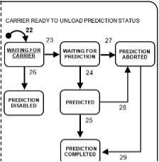
Ballot 7066A proposed changes to the SEMI E87 Carrier Management Services (CMS) standard. This ballot failed previous voting, but now time passed as a ‘superclean’ ballot (no negatives or comments during voting). This ballot included a significant change to the Carrier Ready to Unload Prediction feature which is now called a Carrier Complete Prediction. Anyone who implemented Carrier Ready to Unload Prediction will have to make a lot of changes to comply with the new implementation. A primary driver for this change is to accommodate internal buffer equipment where the READY TO UNLOAD state depends on when the host sends a CarrierOut message and the queue of previously requested activities; therefore, not a useful prediction to make. 

SEMI-Fall-2023-pic1

The benefit of this new state model is to notify the factory host before a carrier is completed so that the automatic delivery can be scheduled to arrive for pickup when the carrier is ready. This can shorten the time it takes for the factory to move material from one equipment to the next. 

Seven similar ballots 7114, 7115, 7116, 7117, 7118, 7119 and 7120 were submitted respectively for standards E5/E30, E40, E87, E90, E94, E116 and E157 to define a ‘well-known name’ for each require collection events, variables and alarms. The ‘well-known’ names are aliases for mapping purposes; necessary because each implementation can use different names. The ultimate goal of this feature is to make the GEM and standards based on GEM more plug-and-play. This new feature serves at least two purposes. Standard E172 already defines a well-known name attribute in the SECS Equipment Data Dictionary (SEDD) file. In the Equipment Data Acquisition (EDA) standard freeze 3 version, E164 will use this well-known name as well. The regular GEM documentation can also reference the well-known name. To explain the value of this feature, E90 requires a collection event for Substrate Location State Model transition 1. Implementers might define this collection event using any name such as E90_Loc_Unoccupied2Occupied, SLTrans1, SubstrateLocationUnoccupiedToOccupied or CollectionEvent901. Any name is allowed. The new well-known name establishes a standardized alias name called the well-known. 

SEMI-Fall-2023-pic2

When ballot 7117 is published, the well-known name table establishes well-known name “E90:SubstrateLocation:001:Unoccupied-Occupied” as the standardized alias for this collection event. This SEDD file can be downloaded through the GEM interface, tell the GEM host exactly which collection event implements the Substrate Location State Model transition 1. During the Information & Control Committee, ballot 7117 resulted in a Ratification ballot handling a long existing E90 naming issue for one status variable. All of the other ballots passed with a simple editorial change. 

A few of the above well-known name ballots included additional line items to resolve issues in the respective standard, mostly editorial or minor. Ballot 7114 included an E5 clarification that Stream 21 Function 17/18 sequence can be aborted by the receiving entity with an S21F0 message. Ballot 7116 included several additional changes/corrections to E87. 

1.    Clarification on the CARRIER SLOT MAP STATUS state SLOT MAP VERIFICATION FAILED, which sometimes was spelled in E87 without the ‘ED’ in FAILED. 
2.    Corrections to Table R1-21 in the table heading.

SEMI-Fall-2023-pic3

3.    Carrier object attribute Capacity can now be format code 51, 52 or 54, increasing the allowed carrier size from 255 to 4.29 GB to accommodate carriers not holding wafers but smaller substrates. 
4.    Carrer state model transition 7 includes a new trigger as already described scenario R1-21. 
5.    Scenario R1-20 was reverted to its original design, undoing an error introduced in 2012

6.    And finally, equipment constant BypassReadID was added to E87.1. This equipment constant has been defined in E87 but missing in E87.1

Ballot 9836 proposed some synchronized changes in E87 and E90 to define new name/value pair attributes. The ballot failed due to some limiting details in the value format definition. The ballot intends to allow equipment and factory to agree to using additional substrate content and characteristic information.

The Japan GEM 300 task force is working on improving the GEM E30 standard. The task force proposed a number of minor improvements mostly editorial to clean up several areas with the specification. Although the work was originally proposed to occur in the North America group, the task force decided to handle this ballot in Japan who will meet in December of 2023. Of course, the regional GEM 300 task forces worldwide all share and vote together on all E30 ballots.

DDA (Diagnostics Data Acquisition) Task Force

The DDA task force reapproved three standards: E128, E138 and 145. Additionally, the DDA task force made more plans to complete the Equipment Data Acquisition (EDA) freeze 3 version. Here are the key activities and findings as of today:

  • E164 will be modified to incorporate the well-known names from the GEM 300 force. Instead of including all GEM 300 standards directly in the E164 primary standard, each GEM 300 standard will have a smaller, simpler E164 subordinate standards (E164.1, E164.2, …) to define the EDA implementation for that standard. This strategy makes adopting EDA and E164 more flexible to use in industries beyond semiconductor front end equipment.
  • Some errors were found in the published .proto files for E132 and E134. New ballots will be submitted as soon as possible to make corrections.
  • A software vendor test #2 will be held immediately following the North America Information & Control Spring meetings. Anyone implementing client and/or server software is invited to attend. Instead of testing for standard compliance, the purpose of the vender test is to test interoperability and flush out any remaining issues in the EDA freeze 3 standards. This software vender test session #2 will focus on previously untested E132 features from software vender test session #1 and will also include E125 tests. Anyone interested in joining should contact me (Brian Rubow) or Albert Fuchigami (Brian’s co-leader). Prior to the software vender test session, the task force co-leaders will provide a test plan document and .proto files with corrections in E132 for known issues.
  • A software vender test session #3 will be held immediately following the North America Information & Control Summer meetings held in conjunction with SEMICON West. This test session will focus on E134 testing. 

ABFI (Advanced Backend Factory Integration) Task Force

Ratification ballots R2924A and R6925A both passed. This means that the new Consumables and Durables standard is in the SEMI publication queue. 

Additionally, ballot 6948 passed with several great improvements to the E142 substrate mapping standard. The improvements should help users better understand how to use the E142 schema files for more consistent adoption by implementers. 

Spring 2024

The next North America Information and Control spring meetings will be held again at SEMI headquarters in Milpitas, California. The dates will be March 25-27, 2024. Although many attendees were remote during these meetings, I expect many more attendees to be in person at these spring meetings due to the EDA software vender test session.  

To learn more about the SEMI Standards and the work we do as members of SEMI, please click the button below.

Contact Us

Topics: Industry Highlights, SECS/GEM, Semiconductor Industry, Smart Manufacturing/Industry 4.0, Cimetrix Products, Standards

How To Use The CCF Communicator Framework To Quickly Develop Device Interfaces

Posted by Sreeraj SA Ambikakumari on Oct 18, 2023 9:54:00 AM

Do you need to develop complex drivers for the components in your equipment? Let’s see how the CIMControlFrameworkTM Communicator Framework helps you accomplish this.

What is the CCF Communicator Framework?

The Communicator Framework simplifies the low-level message handling to and from the hardware by encapsulating the connection between CCF and the device.

As an example, consider how the connection is made between control software and hardware devices. An ASCII serial connection needs a socket connection using TCP, a multi-threaded mechanism to handle multiple messages to/from the devices, logic to synchronize the commands and their respective responses, and several other functions. This is a lot of work when developed from scratch.

As an alternative, CCF provides a built-in ASCII serial connection class to achieve all these quickly. You can simply use this class to create an ASCII serial connection to the component.

What is the specific role of the Communicator Framework?

Each component or device in an equipment provides a set of commands and responses to perform its designated function. The Communicator Framework includes a Transaction class that handles these commands; each command to a particular device is implemented as a transaction.

Consider the case of the Clamp activity for a loadport—the associated command could be “LOCK.” Now let’s see what are our tasks are to implement this command in a loadport driver as a CCF developer.

The first step is to create a Transaction class for the loadport which must be inherited from the base CCF Transaction class. See below for an example that creates the “Clamp” transaction.

CCFCommunicator_image1

In this example, the ClampTransaction class accepts the command Clamp as an attribute. The command which is passed as the attribute to its base class will be sent to the device through the ACSII serial connection.

The next step is to implement a Communicator class to send the command and receive responses from the device. See the sample code below.

CCFCommunicator_image2

The CCF product includes a LoadPort class. Here we initialize the Communicator class with the ASCII serial connection to perform the transaction.

CCFCommunicator_image3

When a clamp activity is needed, CCF calls the Clamp function of the LoadPort to do the clamping. We use the Communicator object just initialized to send the command to the hardware. Note that we did NOT write any code for sending the command or receiving its response because this is the job of the Communicator.  You send the command to the hardware by calling the PerformTransaction function of the Communicator base class as shown below.

CCFCommunicator_image4

Believe it or not… that’s it! We sent a command to the device with very few lines of code in the driver. Now, how do you handle responses from the device? Let’s have a look.

Each device implements different responses to the command set, depending on the manufacturer of that device. This may include acknowledgments, data items, events of various types, and so on. So, whenever the Communicator receives a response from the device, it calls an abstract method on a child class to parse the response. As a CCF developer you must decide what type of response it is, whether or not it successfully completes the transaction, and how to respond to the Communicator as a result.

The example below shows how to parse a response from the device.

CCFCommunicator_image5

Finally, how can we deal with the events from the hardware? From the code above you can see how to indicate that the type of response is an Event, and in this case, it will invoke another abstract method on its child class to handle the event. The CCF developer can then handle it in their code as shown below.

CCFCommunicator_image6

That’s all there is to it. The code segments above provide an example of a basic loadport driver that includes a Clamp transaction.  To implement additional commands for your device, simply add more transactions and call them from the equipment controller. The Communicator Framework will handle the rest of the communication with your device.

To learn more about CCF or other Cimetrix products, click the link below:

Contact Us

Topics: Industry Highlights, Semiconductor Industry, Equipment Control-Software Products, Smart Manufacturing/Industry 4.0, Standards

Information & Control Standards TC China Chapter Summer Meeting 2023 Update

Posted by Eric Zhou on Sep 28, 2023 9:45:00 AM

Backgroundwww.cimetrix.comhubfsStcked_Standards_logo

The China summer SEMI Standards meeting was convened on August 8, 2023 in Shanghai. Two task forces met; the ABFI (Advanced Backend Factory Integration) and GEM300 Task force in the TC China Chapter. I actively participated in both task forces to closely monitor and comprehend all activities discussed during the meeting.

ABFI (Advanced Backend Factory Integration) Task Force

Ballot 7018, one Line Item revision to the SEMI E87-0921, Specification For Carrier Management(CMS) and E87.1-0921, Specification for SECS-II Protocol for Carrier Management(CMS).

It provides a means for the host or equipment to provide the slot map, which contains information regarding the correct and incorrect placement of substrates within a carrier. Additionally, it supports configuration settings that indicate the slot map is not read and will not be verified against host-provided information.  Furthermore, new related roundtrip scenarios are added to Related Information 1 – Carrier Object ID when the equipment lack the hardware for scanning a carrier’s slot map. This ballot was submitted for cycle-2 voting in February 2023 but received three rejections with a total of five negatives. During the ABFI Task Force meeting, we thoroughly reviewed and addressed these negative items.  Consequently, we will revise this ballot accordingly and submit it to the A&R committee for review. 

  1. Line Item #1, Reject from Miyamoto Motoki (Yokogawa)
    • Negative 1 to Line Item #1 :  Accepted and do modification according to negative comments.
    • Negative 2 to Line Item #1-g : Accept and do modification according to negative comments.
  2. Line Item #1 Reject from Matsuda Mitsuhiro (KKR)
    • Negative 1 to Document 7018 Line Item #1:  Negatives is not related with this ballot. This negative was not accepted by Task Force.
    • Negative 2 to Document 7018 Line Item #1:  Negatives is related but not persuasive. This negative was not accepted by Task Force.
  3. Line Item #5 Reject No.1 from Mochizuki Tadashi (TEL)
    • After communication, voter withdrew the reject.

GEM 300 Task Force

In this task force we proposed two SNARFs, one for a line item revision to E40-1218, Specification For Processing Management, and another for E40.1-1218, Specification For SECS-II Protocol For Processing Management, and another for a line item revision to E94-0819R, Specification For Control Job Management and the E94.1-0819R, Specification For SECS-II Protocol For Control Job Management (CJM).
 
Some background information is useful here. In the semiconductor industry, the E90 Specification for Substrate Tracking, E40 and E94 are used together to monitor the substrate and job status in most 300mm frontend and advanced backend factories. Typically, after completing a job, it is the responsibility of the factory host to check the state of all materials to determine if the job has been successfully finished. However, some factories do not track E90 substrate events, and/or certain equipment types lack the capability to report such events. Additionally, some factories believe that the calculation of processed materials, failed materials and  unprocessed materials in a job should be performed on the equipment side, which then provides the final processed results. These factors make it challenging for the factory host to check the process status (processed, failed or unprocessed) of all materials in a job. As more straightforward data reporting requirements have accumulated from various factories, many equipment suppliers have developed their own means for delivering the processed substrate lists and counts. However, due to a lack of reference standards for these requirements and implementations, many variations exist in the data formats used to serve this single purpose.
 
These two SNARFs include revisions as follows to cover the above requirements and gaps:
1. Add new definitions for the Processed, Failed and Unprocessed state of materials.
2. Add a state matrix to better explain the E90 substrate processing states
3. Add new material processing result-related variables for job (process job and control job) events.
4. Add new object attributes for material processing result of job a (process job and control job) objects.
 

Note that these two SNARFs have undergone formal review, and ballots 7139 and 7140 were created as a result.

This blog provides a summary of the deliberations that took place during both task force meetings. For more information about these standards meetings, or questions about Cimetrix, please contact us by clicking the button below.

Contact Us

Topics: Industry Highlights, SECS/GEM, Semiconductor Industry, Smart Manufacturing/Industry 4.0, Standards