Industry News, Trends and Technology, and Standards Updates

European Advanced Process Control and Manufacturing Conference XVI in Review

Posted by Alan Weber: Vice President, New Product Innovations on Apr 19, 2016 2:01:05 PM
APC1.png

APC2.png

Cimetrix participated in the recent European Advanced Process Control and Manufacturing (apc|m) Conference, along with more than 130 control professionals across the European and global semiconductor manufacturing industry. The conference was held in Reutlingen, Germany, a picturesque city of stone and half-timber buildings just south of Stuttgart.

APC3.png

This conference, now in its 16th year, is one of only a few global events dedicated to the domain of semiconductor process control and directly supporting technologies. The conference’s attendance this year was comparable in numbers and demographics to that of the previous two years, a clear indication that this area continues to hold keen interest for the European high-tech manufacturing community. Another highlight this year was the sponsorship of Bosch, a relative newcomer to the conference but a pillar of the German manufacturing industry. Reutlingen is home to Bosch’s automotive electronics division and its related semiconductor manufacturing facilities, so they were very well represented in the conference and excellent hosts!

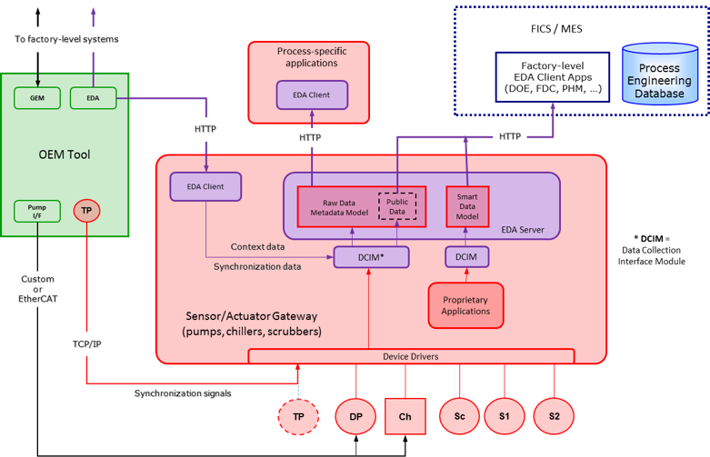
Cimetrix was privileged to make two presentations at this year's conference. The first was entitled “Data Fusion at the Source: Standards and Technologies for Seamless Sensor Integration,” authored and delivered by myself. The external sensor integration and related data unification topics have enjoyed increasing interest over the past year, and even though the techniques outlined in the presentation leverage the latest versions of the Equipment Data Acquisition (EDA)/Interface A standards, they apply equally well for the 200mm manufacturing nodes prevalent in European wafer fabs and assembly/test factories. The solution architecture is shown in the slide below, but for the background and rationale behind this approach, feel free to download a copy of the entire presentation from our website by clicking on the link below.
APC4.png

 Download the Presentation

APC5.png

The second presentation, entitled “'Smart Manufacturing' solutions for high-mix manufacturing using Wait-Time-Waste improvement opportunities” was authored by Jan Driessen, a Principal Industrial Engineer with NXP Semiconductor in the Netherlands. It summarized the work of a project team from six companies and as many countries, and funded by the European Union's “integrate” program (cover page is on the left). Because of an unexpected work conflict during the conference, however, Jan was unable to attend, and, based on our companies’ shared interest in the Wait-Time-Waste technology and standards over the past several years, he thought that Cimetrix would be well qualified to give his presentation. I willingly agreed, worked with Jan to make sure I understood the latest material, and made the presentation. It essentially makes a compelling case for using equipment event data in a legacy 200mm fab to improve OEE, operational effectiveness, and factory capacity through a “chain of data operations” paradigm that he explains in some detail. The good news for 300mm fabs is that these same results can even more readily be achieved, because the availability and fidelity of the event data is much higher, especially if the fab has a full GEM300/EDA E164-compliant system infrastructure. For more information, request a copy of this presentation directly from Jan Driessen at jan.p.driessen@nxp.com.

Other themes that were evident at the conference included 1) applications of APC and supporting metrology techniques for structures found in smart sensors, MEMS devices, LEDs, and other semiconductor products outside the traditional processor and memory segments; 2) increasing emphasis on equipment data collection in the back end to support productivity monitoring and control applications; 3) unit process control for a number of equipment types; and 4) an entire session devoted to industrial engineering topics.

As with other similar conferences around the globe, the takeaway for Cimetrix is that “Smart Manufacturing,” Industrie 4.0, the Industrial Internet of Things (IIoT), advanced process control and fault detection applications, “big data” analytics, and a host of other high-tech manufacturing technologies all depend on the ability to get the right data at the right time from the right sources on the factory floor, and then make it available wherever and whenever needed… For more information about how Cimetrix’s product families that directly address this “sweet spot,” please contact us.

Topics: Industry Highlights, EDA/Interface A, Events

SEMICON China 2016 was the Largest Semiconductor Trade Show of the Last Five Years

SEMICON China SEMICON China

SEMICON China

SEMICON China

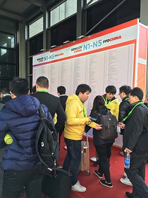
On March 15-17 in Shanghai, SEMI hosted its annual SEMICON China and PFD China, which was the world’s largest semiconductor trade show of the past five years. With an increase of 20% over last year, the show had more than 2,600 booths from companies based all over the world. Many theme pavilions at the exposition demonstrated the strength of the industry. In addition, the series of concurrent conferences and programs brought the global industry knowledge sharing to exhibitors and attendees alike.

Starting Tuesday morning, the Grand Opening Keynote was delivered by world-class industry leaders including Dr. Zhou Zixue—the Chairman of SMIC, Ding Wenwu—the President of China National IC Fund, along with the CEOs from TSMC, Applied Materials, Amkor Technology, TEL, STATS ChipPAC, and Lam Research. The presentation explored global business and technology trends, market opportunities, and shared the panel’s ideas supporting the development of China’s semiconductor industry.

The rapid rise of China’s semiconductor industry has been driven mainly by an increasing market and investments. Chinese companies and funds have been active in the recent cross-border merger and acquisition deals. On Wednesday at the “Tech Investment Forum – China 2016,” leaders of China’s IC Investment Fund and leading global investment institutions discussed investment hot-topics within the Chinese semiconductor industry.

Also on Wednesday, SEMICON hosted a “Build China IC Manufacturing Ecosystem” forum that discussed establishing a full integrated circuit (IC) manufacturing supply-chain and building manufacturing core competencies that are vital for China’s semiconductor industry. The forum included speakers from China and leading global companies from the IC design, manufacturing, equipment, and materials fields. A wide range of topics was  covered including innovation and cooperation in leading-edge frontend processes, advanced packaging technologies, eight-inch production line, and more.

Other concurrent technology sessions included “China Memory Strategic Forum,” “Technology Shape the Future – Senor Hub Solution for Wearable and IoT,” “LED China Conference 2016,” “Power Semiconductor Forum 2016,” “SEMI-JEDEC Mobile and IoT Technology Forum,” and “China Display Conference/ASID 2016.” These sessions illustrate how the Chinese semiconductor market is interested in exploring industrial developments, share its visions for the future, and to work cohesively to grow the industry within China.

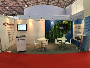
This was the first year Cimetrix exhibited at SEMICON China. We were able to make some valuable connections, visit with existing customers, and establish that Chinese companies have a definite interest in our product lines as well as how we can help them find greater success. We featured our complete SECS/GEM and EDA product lines with in-booth demonstrations and presentations.

We have already made plans to attend next year’s show to further explore how we can fit into the expanding Chinese market. We are hopeful that China will open new possibilities for the continued growth of Cimetrix.

Topics: Semiconductor Industry, Doing Business with Cimetrix, Events

SEMICON Japan 2015 Spotlights IoT and its Effects on the Semiconductor Industry of the Future

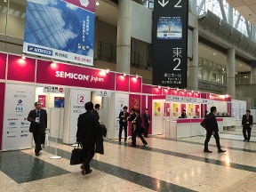
December 16-18 in Tokyo, SEMI played host to SEMICON Japan that was co-located with the WORLD OF IOT, a special “show-within-a-show” dedicated to the Internet of Things usages that are propelling the next generation of microelectronic advances. SEMICON Japan is of note as Japan has the world’s largest installed fab capacity with more than 4.1 million 200mm equivalent wafers per month representing a high product mix.

Over 60,000 visitors attended the three-day event who met with nearly 800 exhibitors; attended forums, technical sessions, and networking events; and had the opportunity to see new innovations and technologies within the industry.

semicon japan.jpg

Semicon Japan

Semicon Japan

One highlight of the show was the Sustainable Manufacturing Pavilion. The pavilion focused on 200mm fab capacity where increased demand from IoT devices is anticipated. Revamping of the existing capacity and building cost-conscious capacity will be key to the sustainable growth of the industry. Sustainability in microelectronics manufacturing is quickly moving from a minor area of focus to a major consideration in business planning. Forward-thinking device makers, materials suppliers, and equipment manufacturers are all beginning to understand sustainable manufacturing makes economic sense for the future.

The pavilion offered many related sessions throughout SEMICON including the SEMI Technology Symposium Test Technologies for Automotive Semiconductors; the SEMI Technology Symposium on DFM in the Trends towards Fabless/Foundry Manufacturing and Alliances; the SEMI Technology Symposium on The Dreams and Reality of TSV/2.5D/3D Packaging; and a Sustainable Manufacturing and High Tech Facility Forum.

This year’s SEMICON Japan also featured a Manufacturing Innovation Pavilion that showcased inventive processes, equipment, manufacturing, components, and materials technologies that enable smarter and faster—yet cheaper—semiconductor devices to create our advancing society, industry, and life. The pavilion demonstrated that developing microelectronics technologies that will make the IoT possible requires continued innovation in semiconductor manufacturing equipment, materials, and components.

In conjunction with the Manufacturing Innovation Pavilion, SEMICON conducted a Semiconductor Executive Forum, a Lithography Business Forum, and a Manufacturing Innovation Forum to exchange ideas and share knowledge about the topics featured in the pavilion.

The WORLD OF IOT brought together leading global electronics and microelectronics companies whose innovations are driving the expansion of mobile technologies, cloud computing, and network-connected devices. Held in conjunction with SEMICON Japan, WORLD OF IOT was a "show-within-a-show". Exhibitors included such noteworthy companies as Tesla Motors, Toyota Motor Corporation, and Intel KK that demonstrated current projects and developing technologies. Executive forums and technical sessions were also offered everyday during the show.

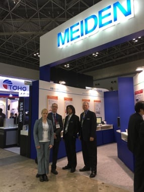
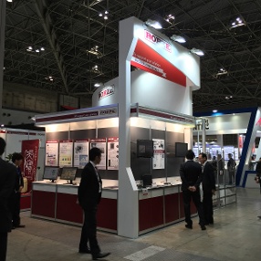
Cimetrix was proud to be represented by our two distributors in Japan, Meidensha Corporation and Rorze Corporation, who both featured our SECS/GEM and EDA product lines. For Rorze, 2015 has been a significant year, the company celebrated its 30th anniversary. Stay tuned for my upcoming blog about its amazing anniversary celebration.

SEMICON Japan 2015 made a great end cap to the year as it focused so heavily on where the semiconductor industry is headed. Hopefully all the SEMICONs in 2016 will continue to be forward-looking as we here at Cimetrix are and remain focused on seeing how managing big data is becoming an ever more important issue within manufacturing. For more information on how EDA/Interface A is equipped to manage data acquisition in fabs, click here.

Topics: Semiconductor Industry, EDA/Interface A, Partners, Events, Data Collection/Management

2015 Advanced Process Control (APC) Conference Focused on High Quality Equipment Data

Posted by Alan Weber: Vice President, New Product Innovations on Oct 23, 2015 1:00:00 PM

01_Flags_above_Austin.jpg

02_APC_Conference_Banner.jpg

03_Jalepenos.jpg

04_APC_Conference_Agenda_Cover.jpg

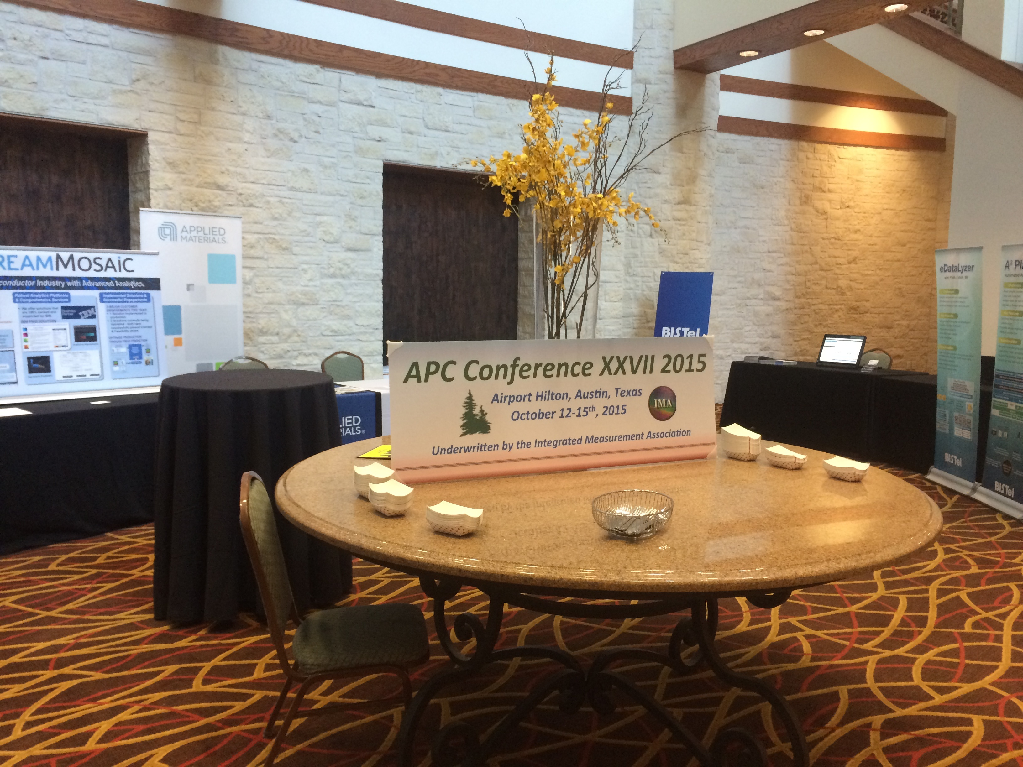
Cimetrix participated in the recent Advanced Process Control (APC) Conference in Austin, Texas, along with more than 120 control professionals across the semiconductor manufacturing industry. This conference, now in its 27th year, is one of only a few global events dedicated to the domain of semiconductor process control and directly supporting technologies, so it was encouraging to see its attendance and energy level rebound from its low water mark a few years ago. The calendar may have indicated it was fall, but nobody told the weather forecasters… Austin set temperature records that week, even hitting 99°F one day!

Given the importance of high quality equipment data for all types of equipment- and factory-level process control applications, it is vital that Cimetrix and its customers understand the current requirements and future direction of this industry segment. Many presentations addressed these topics indirectly, but perhaps the newest insights in this regard came not from the wafer fabrication processes, but rather from the Back End, OSAT (Outsourced Assembly and Test), and advanced packaging segments.

As evidence, a number of presenters mentioned the growing need for equipment data collection in these areas, and cited the following reasons: 1) increasing demands by the consumer product manufacturing customers of these facilities (especially smart phone providers, but others as well) for equipment data to support their product quality and supply chain optimization initiatives; 2) emphasis on the Overall Equipment Effectiveness (OEE) productivity metrics, and the event/status data needed to support their automated calculation; 3) broader deployment of multi-variate Fault Detection and Classification (FDC) applications, which require more equipment trace data parameters than have typically been collected from back end equipment; and finally, 4) actual feedback control based on back end metrology – the best example of this presented last week was an application on dicing equipment that showed how kerf data collection and analysis can be used to adjust saw process parameters

The takeaway for Cimetrix in all this is that the back end equipment suppliers will need to anticipate this demand and may need to upgrade their interface capabilities substantially.

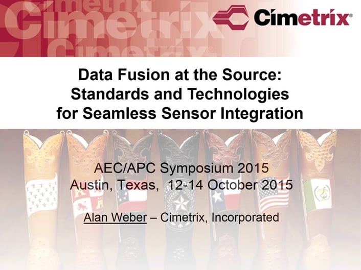
Since some of Cimetrix’ customers have pioneered the application of the latest generation of SEMI EDA (Equipment Data Acquisition) / Interface A standards in plumbing data from external “add-on” sensors to fault detection applications, I presented a generalization of this approach during one of technical sessions. This presentation, “Data Fusion at the Source: Standards and Technologies for Seamless Sensor Integration” is available on the Cimetrix website for those who want to learn more about how this is done.

05_Weber_Presentation_Cover.jpg       Download Presentation  

Check back next week to learn more about creating good EDA/Interface A purchasing specifications.

Topics: EDA/Interface A, Events, Data Collection/Management

SEMICON Europa 2015 Offers Insights into Upcoming Trends in the Semiconductor Industry in Europe

This week Cimetrix exhibited at SEMICON Europa 2015 along with about 400 other companies in the semiconductor industry in Dresden, Germany. The leading trade fair offered a chance for members of the industry to learn about new topics, information, and opportunities to help support and further develop the semiconductor industry across Europe.

An estimated 6,000 were in attendance at this SEMI-sponsored event. Some of the highlights of the three-day event were:

  • The Industry 4.0 Session: The term "Industry 4.0" has been established to describe the penetration of information science into manufacturing forming the next industrial revolution. The TechArena provided information about different aspects of this process.

  • The Emerging Research, Materials and Processes Session: The nanoelectronics research community is continuously exploring a range of new materials to enable further scaling of semiconductor devices and associated technologies, as well as many potential methods to create these materials with methods that allow utilization for future technology nodes. In this session several of these new materials and process developments were discussed by experts in their specific fields. Focus was on the unique properties of the materials or processes, what makes them specifically suitable for targeted applications, how they are characterized and/or how they can be fabricated. Among the topics that were presented were the newest developments for GaN processing, two-dimensional semiconductors devices and fabrication, metal organic frameworks as low-k materials, advanced memory materials such as FeRAM or MRAM Spintronics, and Selective Atomic Layer Deposition.

  • The Semiconductor Technology Conference (STC): This conference explored the efforts of our industry to ensure productivity enhancements for future advanced technology nodes, considering both a wafer size transition, and a continuation of current state of the art and smaller wafer sizes. Updates from around the world on wafer size transition activities were heard and there was a dedicated focus on “beam-based” metrology activities from METRO450 in Israel. SEMI invited their partners to share with attendees their insights, activities, and results in the preparation of future offerings of process equipment, materials, IT/fab automation systems, facilities and fab infrastructure, in order to rise to the challenge to ensure a continued economic manufacturing of state of the art semiconductor chips.

This year we exhibited as part of Silicon Saxony's Industrie 4.0 booth that consisted of about 40 kiosks representing companies with varying focuses within the industry. On Wednesday night, Silicon Saxony played host to all of the booth's exhibitors in a "Countries of Europe"-themed party. The event gave the Cimetrix team a chance to catch-up with friends and colleagues, and discuss new business opportunities. We'd like to thank Silicon Saxony for the great networking opportunity.

We are looking forward to SEMICON Europa 2016 in Grenoble, France next October and hope to see you there. If you didn't get a chance to meet with Cimetrix in Dresden this week and you would like to learn more about our complete line of factory connectivity and equipment control software solutions, please click here

Topics: Semiconductor Industry, Events, Smart Manufacturing/Industry 4.0

SEMI Standards Meetings from the North American Information & Control Committee Forecasts the Direction of the Semiconductor Industry

Posted by Brian Rubow: Director of Solutions Engineering on Sep 29, 2015 1:30:00 PM

During the week of SEMICON West in San Francisco this past July, the North American Information & Control Committee met to discuss and consider new and pending standards within the industry. SEMATECH was noticeably absent from the sessions. For many years, SEMATECH has been a leader in developing and promoting the GEM 300 and EDA standards.

Here are the highlights from those meetings and how they will effect you.

The DDA Task Force is in the early stages of planning a Freeze 3 version of the EDA (Interface A) standards. This may cause some concern—especially with OEMs—as some are just now getting their Freeze 1 interfaces accepted in Fabs. Freeze 2 was a big step forward in making the standards clearer and easier to adopt, but it required a lot of work to move from Freeze 1 to Freeze 2. The hope is that the transition from Freeze 2 to Freeze 3 will be easier, but there will be doubt and concern among many OEMs.

One of the changes proposed for Freeze 3 is replacing the usage of SSL (HTTP) with WS-Security, an extension to SOAP and a member of the web services specifications published by OASIS. This extension allows for secure data within a SOAP message, while still using HTTP for data transfer. This is really an underlying issue and should not affect the applications that would interface with our CIMPortal Plus product. It would allow for a secure connection between CIMPortal and the Fab client so that the data transmitted is protected from theft. There would be configuration changes required to allow the secure connection to be defined, but—once it is—the actual interaction between the OEM’s application and CIMPortal Plus should not change.

Another change being considered is the implementation of WS-ReliableMessaging, another extension to SOAP and also a member of the web services specifications published by OASIS. WS-ReliableMessaging describes a protocol that allows SOAP messages to be reliably delivered between distributed applications in the presence of software component, system, or network failures. Just as the WS-Security item above, this would be at the protocol level, an “under-the-hood” change. It should not affect the way applications interact with our product, but should provide for a more reliable connection to the host EDA client. Use of this extension could also allow EDA to be used in more factory applications, where guaranteed data acquisition is required.

The final issue that was discussed relating to Freeze 3 was a new high-frequency trace for collecting data at very high speeds triggered for short periods of time where the collected data is sent at the end of the collection period. For example, a 1 ms trace for 5 seconds where the 5,000 collected samples for each parameter would be sent at the end of the 5 second period. This change might require alterations in our products. This will help the data reporting be more efficient. Rather than reporting small individual pieces of data to the EDA client, this will allow many data samples to be sent together making for more efficient use of the network.

The GEM 300 Task Force had three ballots on hold due to the ongoing SML copyright legal trial between SEMI and The PEER Group. However, work on other pending ballots continued. The first, Ballot 5872, proposes to add new features to the E172 SEDD standard. E172 is a new standard that provides an XML schema for documenting a GEM/GEM 300 interface. Eventually, E172 can completely replace the current GEM documentation requirements.

Recipe Integrity ballot 5618 has an uncertain future since ISMI failed to pursue its development; unfortunately, the ballot had seemed very close to completion. This standard says that it will not require changes to SECS II messages, but simply clarifies what parameters are defined and how the existing pieces work together. So, essentially, it would be a standard that tells you how to use other existing standards.

Finally, the Task Force discussed enhancing the GEM 300 standards to handle equipment that bond substrates and divide substrates. This will affect E90 and could affect E40, E87, and E94 as well. These changes would likely require updates to CIM300. Right now the standards just address how to treat equipment where the same material (substrates or wafers) go in and out. Traditional material tracking assumes one wafer in, get processed, then return to an output carrier. In the proposed case, either two wafers go in and one unit comes out, or one substrate goes in and two come out

The committee is scheduled to next meet in November, so you can plan on seeing another post from me on the outcome of those meetings afterwards. Subscribe to our blog in the upper right corner of this page to be sure not to miss that or any of my future updates on the North American Information & Control Committee.

Topics: Industry Highlights, Semiconductor Industry, EDA/Interface A, Events

2015 SEMICON Taiwan Recap

Posted by Alan Weber: Vice President, New Product Innovations on Sep 8, 2015 9:41:00 AM

The 2015 SEMICON Taiwan was held at the Taipei Nangang Exhibition Center in the Nangang District of Taipei City, Taiwan September 2-4.  The event drew over 30,000 visitors from all over the world for the three-day event with nearly 1,500 exhibits from a diverse array of companies and organizations across the semiconductor industry.

Blog_pic_2_-_booth.jpg

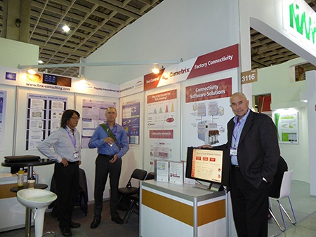
Cimetrix exhibited at SEMICON Taiwan trade show for the first time, in conjunction with its newest Asian partner, Flagship International.

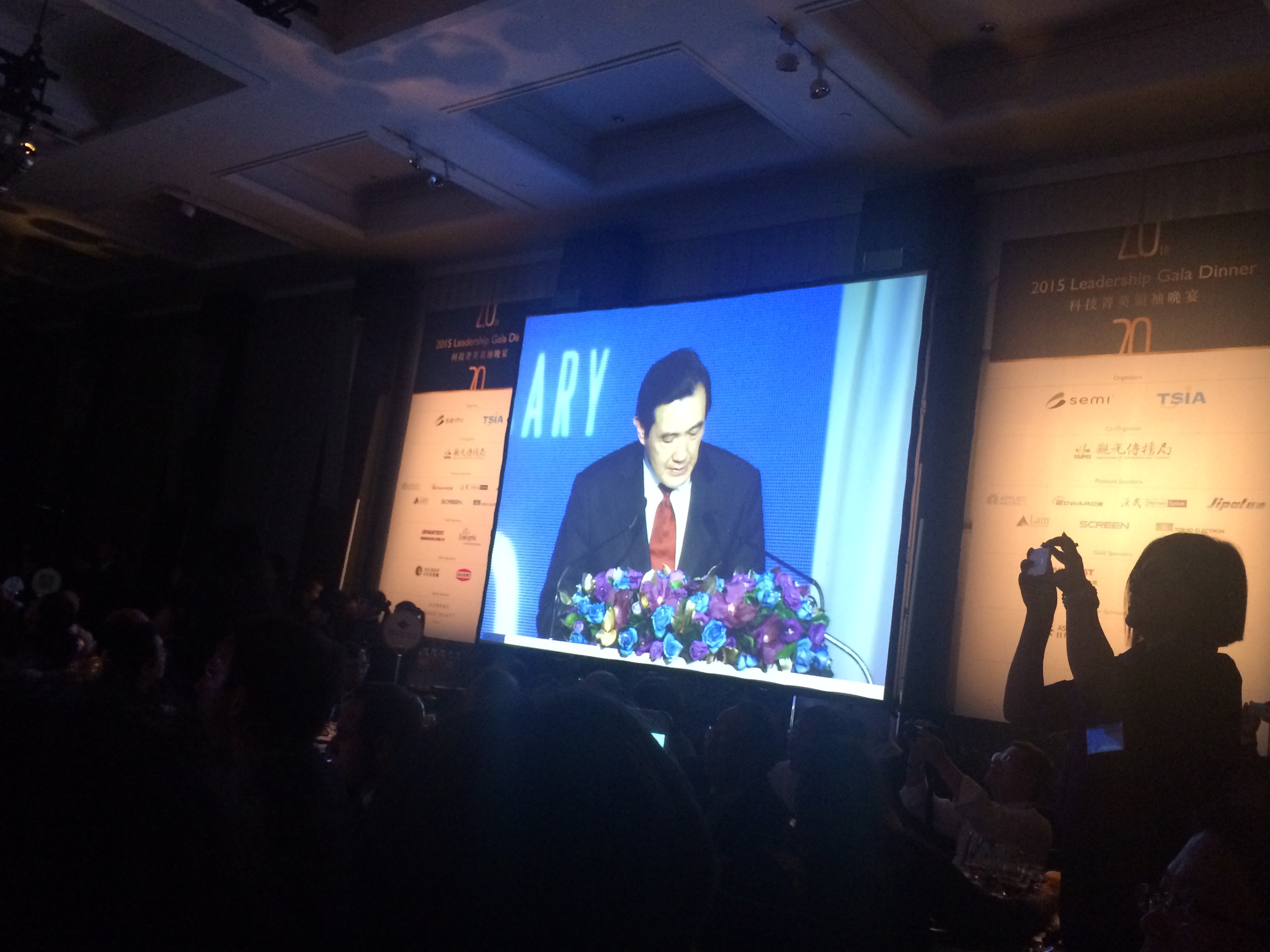
This turned out to be the 20th Anniversary of SEMICON Taiwan, so the mood was especially buoyant and the attendance brisk. SEMI also commemorated the event with a Gala Dinner at the Grand Hyatt on Wednesday night, and we were privileged to attend courtesy of our Flagship colleagues.

The president of Taiwan, Ma Ying-jeou, even made a guest appearance to thank the semiconductor industry for its contribution to Taiwan’s economic health. 

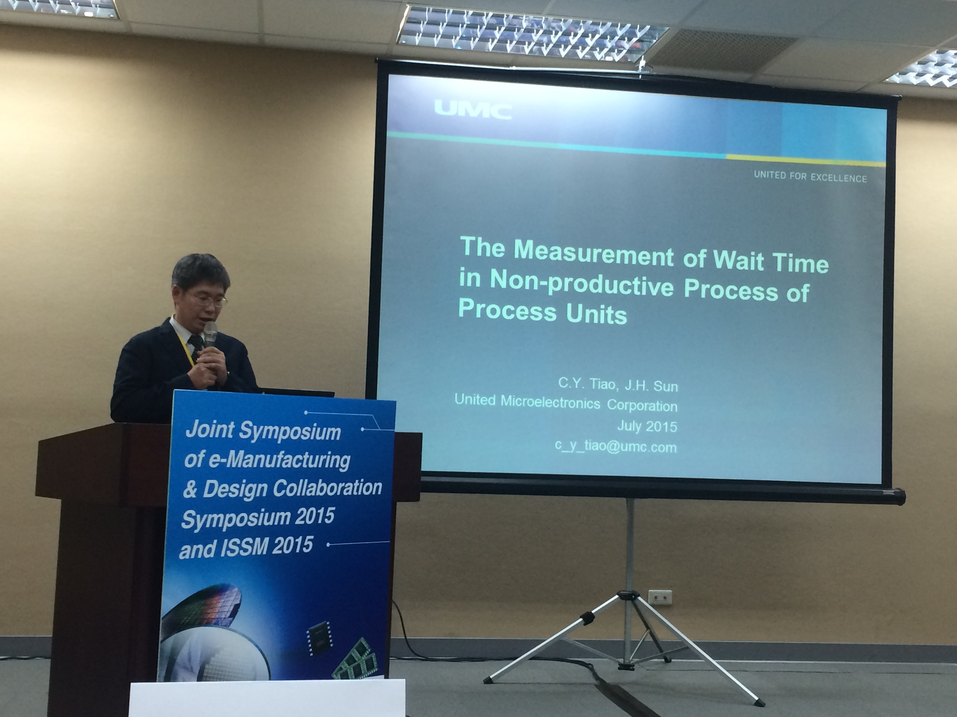
Shortly after the exhibition opened on Wednesday (Sept. 2), a couple of visitors from UMC showed up, and shared the latest work they’ve been doing with the Wait Time Waste (WTW) concepts that we had presented two years earlier. C.Y. Tiao and James Lin of UMC even made two presentations at the eMDC conference on this topic. 

From a standards perspective, this has now taken the form of SEMI E168, Specification for Product Time Measurement (PTM), and has been defined at the “time element” and supporting GEM/SECS message level for process equipment, automated material handling systems (AMHS), and material control systems (MCS). With the advent of SEMI E164 (EDA Common Metadata), these concepts are especially easy to implement, because all the events necessary to calculate the full suite of time elements are required by standard… but more on this is a later blog!

Since much of the world’s foundry capacity is in Taiwan, the equipment industry was well represented at the show, which included many of Cimetrix’ current customers as well as a few local prospects. As a result, Dave Faulkner and Kerry Iwamoto had a chance to visit a number of these firsthand.

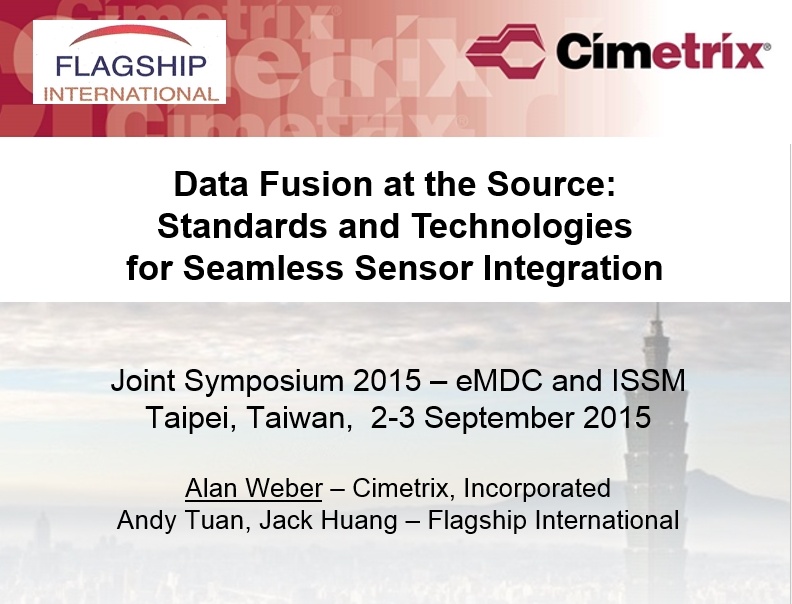
Another highlight of the week for Cimetrix was participation in the eMDC (e-Manufacturing & Design Collaboration Symposium), where I made a presentation entitled “Data Fusion at the Source: Standards and Technologies for Seamless Sensor Integration” that addresses the challenges faced by process engineers in effectively using data from an increasing number of sources to analyze process behavior.

The basic idea is to handle the association of necessary context information (lot, substrate, product, layer, process, recipe, step, chamber, etc.) with the raw collected data as close to the source as possible, using a single, integrated model of the equipment and all related data sources. The equipment model that forms the foundation of the EDA/Interface A standards serves this purpose perfectly.


On a final related note, in visiting and talking with a number of the leading chip makers during the week, it seems that the adoption momentum for EDA is now building steadily, so we look forward to supporting this initiative across the value chain. Stay tuned for a late September post that will shed more light on this process!

Topics: SECS/GEM, Semiconductor Industry, Events

SEMICON Japan 2014

It was exciting to be at SEMICON Japan a couple of weeks ago. The show was in a new venue – Tokyo Big Sight; in previous years, it had been at the International Exhibition Halls & International Conference Hall in Tokyo.


Tokyo_Big_Sight

Tokyo Big Sight

I was especially interested in seeing some of our equipment supplier customers, since we have several new customers who have completed their systems and will ship products using Cimetrix software in 2015 using both our Interface A and SECS/GEM software.

We were well represented at the show. We had a large presence in the booths of our distributors in Japan.

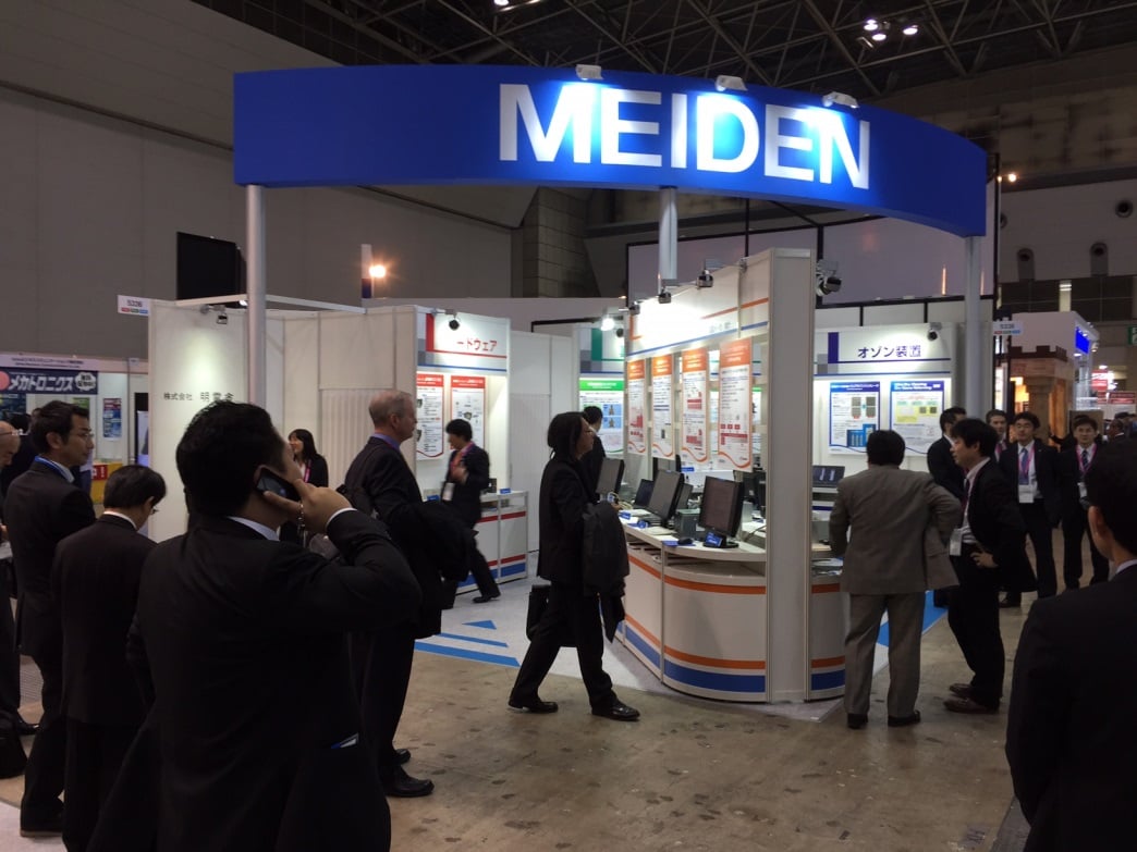
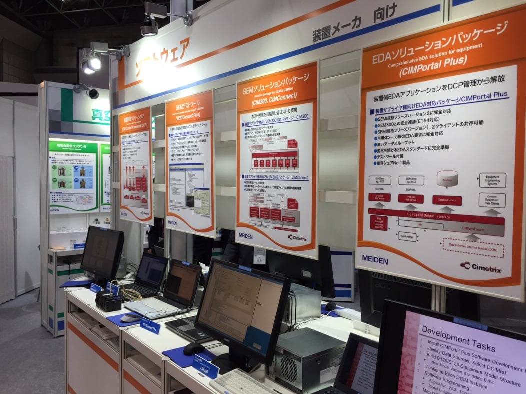
Meiden_Booth_1


Meiden_Booth_2

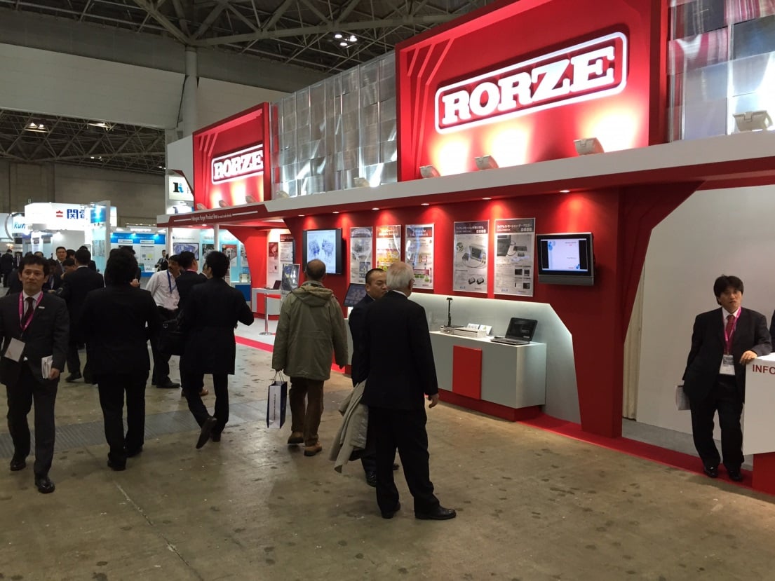
Both Meidensha and Rorze had banks of computers set up to demonstrate Cimetrix software, and both booths were busy with demos.

Rorze_Booth

SEMICON Japan was first held in 1977, and is the largest of the SEMICON events held worldwide each year. This year, there were forums covering subjects such as:

  • Recent advances in 2.5D/3D ICs
  • TSVs in 2.5D and 3D
  • IoT (Internet of Things) and its application
  • Advanced Lithography
  • Design For Manufacturing (DFM)

You can read more about the event at SEMICON Japan.

Topics: Partners, Events, Global Services

2013 SYSTEMA Expert Day - Solutions for Semiconductor Manufacturing

Posted by Cimetrix on Apr 2, 2013 9:15:00 AM

by Alan Weber

Director of Value-Added Products

Advanced Software Solutions for Equipment Health and Productivity Monitoring

On April 18, 2013, SYSTEMA GmbH and Cimetrix will host the second SYSTEMA Expert Day 2013 in Dresden, Germany. The focus will be on advanced software solutions for equipment health and productivity monitoring in the discrete manufacturing industries.

SYSTEMA chose the time and place for this event to make it convenient for attending the 2013 European APCM Conference, which will be held at the Dresden Hilton on April 15-17. 

There will be presentations from industry experts across the semiconductor supply chain, including semiconductor manufacturers, equipment suppliers, and software products and services suppliers.

Monitor

The topics will address equipment-related challenges facing semiconductor manufacturers, and there will be discussions and demonstrations regarding:

  • The best practices in data collection
  • Fingerprinting  - equipment  health monitoring and fault diagnosis
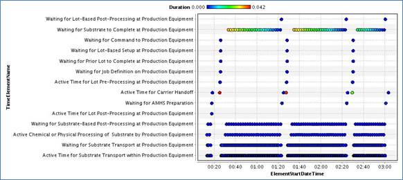
  • Wait Time Waste reduction using substrate-level equipment productivity tracking and analysis.

Wait Time Waste Monitor 

The agenda as it is currently:

 Time

 Topic

 Speaker

8:30 – 9:00

 Registration


9:00 – 9:15

 Welcome & Introduction

 Ricco Walter, SYSTEMA  GmbH

9:15 – 10:00

 Metadata Standards, Equipment Modeling, and  Conformance Testing

 Alan Weber, Cimetrix

10:00 – 10:30

 From Equipment Signals to Quality Information

 Roland Willmann, acp-IT

10:30 – 11:00

 Break


11:00 – 11:30

 Emerging Best Practices in Equipment Professional  Services

 David Grimes, TEL  Europe

11:30 – 12:00

 Identifying Throughput Time Issues –
 Use Cases in  Tool Productivity Monitoring

 Alan Weber, Cimetrix

12:00 – 13:30

 Lunch and Panel Discussion:
 “Future Directions in Equipment Data Analysis"

 Speaker Panel

There may be changes to the agenda, so check the SYSTEMA web page for the event for more details (see the link below).

The people who will get the most out of these presentations and discussions are

  • Equipment and process engineers
  • Field service engineers and system integration specialist
  • Advanced process control specialists
  • Automation technology developers and automation software product managers

Topics: Partners, Doing Business with Cimetrix, Events

Presenting New Cimetrix Products in Japan

Posted by Cimetrix on Jan 7, 2013 10:44:00 AM

By Dave Faulkner

Executive Vice President, Sales and Marketing, Cimetrix

SEMICON Japan 2012 was a great experience, and it was amazing to see the excitement and interest in new developments as the industry prepares for growth in 2013. We were able to showcase Cimetrix products at the booths of Meiden and Rorze, our distributors in Japan. We also displayed CIMControlFramework in the MKS Instruments booth.


SCJapan 2012 logo 0212 EN 2 resized 600


Meiden and Rorze demonstrated CIMPortal 2 for the many OEMs we have in Japan currently using CIMPortal 1.x.  CIMPortal 2 provides the tools for equipment companies to comply with the SEMI E164 standard when they are implementing an EDA/Interface A connection. The E164 standard, approved by SEMI this year, was developed so that companies using EDA/Interface A connections can generate a more consistent and high-quality definition of their equipment’s model, as represented in the metadata file. The CIMPortal 2 toolkit includes many features that reduce development time and effort, including a drag-and-drop equipment model builder and compliance checker.
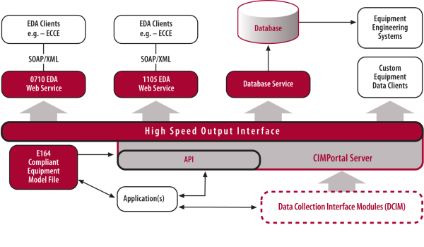
CIMPortal Architecture
We also presented and demonstrated the Wait Time Waste (WTW) and Fingerprinting projects we are developing in collaboration with ISMI. Due to an emphasis on productivity improvement demands, many semiconductor fabs are very interested in hearing about how they can reduce costs using the WTW metrics and methods in development. Fabs are also interested in fingerprinting – also known as equipment health monitoring – in order to reduce the time to repair equipment and avoid downtime. Alan Weber, Director at Cimetrix, taped a presentation and demonstration of fingerprinting that was shown in the Meiden and Rorze booths.

We also highlighted our CIMControlFramework equipment software framework at the Meiden, Rorze, and MKS Instruments booth. OEMs are looking for an equipment control software solution they can use for high-volume applications, and they like the concept of being able to manage the development in-house. By using a flexible, extensible, configurable framework, OEMs can implement custom extensions for new customers and design the next generation of system internally, allowing them to maintain control of their own development process. Rorze now offers not only CIMControlFramework as a stand-alone product, but also packaged with robot hardware including EFEMs and Vacuum Platforms.

Kerry Iwamoto, the Managing Director of Cimetrix Japan K.K., and I presented at the SEMI Productivity Standards Workshop, which focused on Wait Time Waste. This workshop, which was one of the better-attended sessions, presented new proposed standards development activities to improve manufacturing productivity and reduce costs. Kerry and I described plans for developing a SEMI standard for Wait Time Waste methods and metrics that will allow semiconductor fabs to measure product wait time and use that data to reduce waste and cycle time. We showed how the WTW Reference Implementation (WTWRI) developed by Cimetrix can help fabs pinpoint process delays and determine how to reduce them.

Japan is going through some tough times both politically and in their semiconductor industry. But now is the time to work closely with high volume OEMs in Japan as they retool their strategy for the next phase of semiconductor growth.

Topics: Events, Cimetrix Products