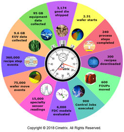
 We introduced the Giga Factory Minute concept last year to highlight the impact that standards have in orchestrating the entire manufacturing process, from releasing unpatterned wafers into the line (1:00 on the figure) to the shipment of good die to the downstream assembly/test facilities (12:00). This year, we’ll use this same diagram to identify important industry trends, technologies, events, or other items of interest to our subscribers. Since there are 12 “hours” on the diagram, watch for a posting every month related to the topic in that segment.
January 2019
Since this is January, we’ll focus on the more general topic of electronics manufacturing product materials, of which “wafer starts” is the specific material type that begins the 4-month journey through the wafer fab.
In the early days of the automated factory industry, there were only a few material form factors to deal with… even when you go all the way back to the raw silicon and forward to the finished electronic product. (You can see most of these on the “Sand to Systems” infographic here.)
However, now that semiconductors have found their way into virtually every major industry on the planet, from computers to entertainment to transportation to agriculture to wearables and even to “ingestibles,” the automated material handling challenges across this product diversity have exploded. And it’s only going to get worse. 
You may not be responsible for handling exotic material types anytime soon, but understanding the role that equipment connectivity standards can have at the earliest steps in a Smart Manufacturing process is useful nevertheless. Give us a call if you’d like to know more about how these technologies can benefit your operations.


