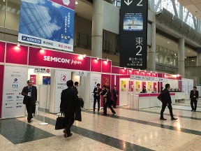
December 16-18 in Tokyo, SEMI played host to SEMICON Japan that was co-located with the WORLD OF IOT, a special “show-within-a-show” dedicated to the Internet of Things usages that are propelling the next generation of microelectronic advances. SEMICON Japan is of note as Japan has the world’s largest installed fab capacity with more than 4.1 million 200mm equivalent wafers per month representing a high product mix.
Over 60,000 visitors attended the three-day event who met with nearly 800 exhibitors; attended forums, technical sessions, and networking events; and had the opportunity to see new innovations and technologies within the industry.


One highlight of the show was the Sustainable Manufacturing Pavilion. The pavilion focused on 200mm fab capacity where increased demand from IoT devices is anticipated. Revamping of the existing capacity and building cost-conscious capacity will be key to the sustainable growth of the industry. Sustainability in microelectronics manufacturing is quickly moving from a minor area of focus to a major consideration in business planning. Forward-thinking device makers, materials suppliers, and equipment manufacturers are all beginning to understand sustainable manufacturing makes economic sense for the future.
The pavilion offered many related sessions throughout SEMICON including the SEMI Technology Symposium Test Technologies for Automotive Semiconductors; the SEMI Technology Symposium on DFM in the Trends towards Fabless/Foundry Manufacturing and Alliances; the SEMI Technology Symposium on The Dreams and Reality of TSV/2.5D/3D Packaging; and a Sustainable Manufacturing and High Tech Facility Forum.
This year’s SEMICON Japan also featured a Manufacturing Innovation Pavilion that showcased inventive processes, equipment, manufacturing, components, and materials technologies that enable smarter and faster—yet cheaper—semiconductor devices to create our advancing society, industry, and life. The pavilion demonstrated that developing microelectronics technologies that will make the IoT possible requires continued innovation in semiconductor manufacturing equipment, materials, and components.
In conjunction with the Manufacturing Innovation Pavilion, SEMICON conducted a Semiconductor Executive Forum, a Lithography Business Forum, and a Manufacturing Innovation Forum to exchange ideas and share knowledge about the topics featured in the pavilion.
The WORLD OF IOT brought together leading global electronics and microelectronics companies whose innovations are driving the expansion of mobile technologies, cloud computing, and network-connected devices. Held in conjunction with SEMICON Japan, WORLD OF IOT was a "show-within-a-show". Exhibitors included such noteworthy companies as Tesla Motors, Toyota Motor Corporation, and Intel KK that demonstrated current projects and developing technologies. Executive forums and technical sessions were also offered everyday during the show.
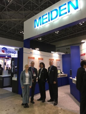
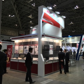
Cimetrix was proud to be represented by our two distributors in Japan, Meidensha Corporation and Rorze Corporation, who both featured our SECS/GEM and EDA product lines. For Rorze, 2015 has been a significant year, the company celebrated its 30th anniversary. Stay tuned for my upcoming blog about its amazing anniversary celebration.
SEMICON Japan 2015 made a great end cap to the year as it focused so heavily on where the semiconductor industry is headed. Hopefully all the SEMICONs in 2016 will continue to be forward-looking as we here at Cimetrix are and remain focused on seeing how managing big data is becoming an ever more important issue within manufacturing. For more information on how EDA/Interface A is equipped to manage data acquisition in fabs, click here.♦


