Industry News, Trends and Technology, and Standards Updates

History of Semi Equipment Health Monitoring - Fingerprinting

Posted by Alan Weber: Vice President, New Product Innovations on May 31, 2013 3:12:00 PM

I had the privilege of speaking at the annual Advanced Process Control and Manufacturing (APCM) Europe conference in April of this year. The conference supports manufacturers, suppliers and scientific community of semiconductor, photovoltaic, LED, flat panel, MEMS, and other related industries. The topics are focused on current challenges and future needs of Advanced Process Control and Manufacturing Effectiveness. The theme of this year’s conference was From Reactive to Predictive - from SPC to Model-Based Process Control.

My presentation was entitled Fingerprinting and FDC: First Cousins in the Equipment Productivity Family. One of the areas I covered in that presentation was how the whole concept of fingerprinting came about.

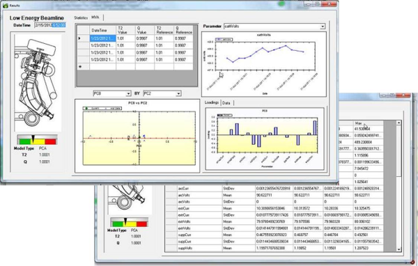
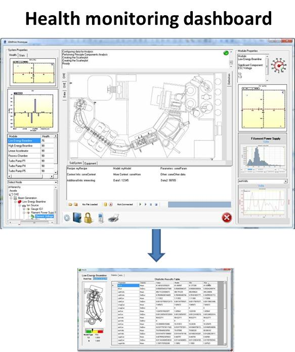
I’ve written about Equipment Health Monitoring, also known as fingerprinting, previously – see my blog post about Fingerprinting at SEMICON West at SEMICON West Follow Up: ISMI Fingerprinting Project. While the term fingerprinting has only recently been applied to this technology, the use of this type of application goes back a decade to the advent of Equipment Engineering Systems (EES), when the first major implementation of that technology was in the Renesas factory in Naka, Japan.

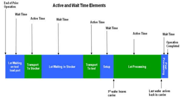
The basic idea was that semiconductor manufacturers could learn a great deal by collecting detailed trace and event information from the equipment to understand the behavior of low-level mechanisms, with the assumption that if the low-level mechanisms were exhibiting proper behaviors, then the entire machine would be operating within its specifications. This is the fundamental idea behind fingerprinting.

 Fingerprinting History

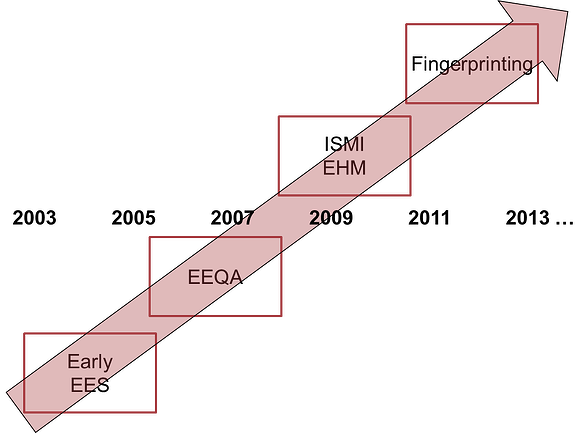
Back in 2003, when Renesas was implementing their EES program, there were no good standards for collecting low-level, high-speed trace information, and so the Renesas engineers expended a great deal of effort generating custom interfaces to collect trace and event data they could then feed into a common database. However, as they pursued the effort, they showed what kinds of analysis of the collected data could give them insight into the performance of their fab’s equipment.

As this idea gained traction, Shigeru Kobayashi one of the industry thought leaders at Renesas, proposed through the ITRS and SEMATECH to create a program around the idea of using detailed trace information to improve the equipment quality over time. This suggestion triggered the inception of the EEQA (Enhanced Equipment Quality Assurance) program.

The basic idea of the EEQA program, as it was with EES, was to collect low-level trace information about equipment mechanisms. That data could be shared with the equipment suppliers to show them how the equipment was operating in a production situation in order to improve the design and performance of the machines over time.

The EEQA program lasted more than 3 years at ISMI. There were a number of studies regarding the specific information that equipment engineers and fab engineers could use to characterize different equipment mechanisms and components. There were even a couple of prototypes developed to show how that information could be collected, modeled, and visualized and reported. However, the structural problem with the program was that it placed expectations on the OEMs regarding the amount of data that would need to be collected (and the effort involved in enabling this) without clearly showing the benefit to these suppliers. Consequently, the EEQA program lost support and lay fallow for a while.

However, the basic ideas of EEQA were preserved and folded into a subsequent SEMATECH umbrella program called equipment health monitoring (EHM). However, the energy for the program happened when someone attached an intuitive label to this notion of characterizing a component with its raw data. People attached the term “fingerprint” to that basic model, and the idea of grouping these trace values into a fingerprinting model that would have a specific value that manufacturing can track over time made the basic idea easier to understand and support. When EEQA was re-characterized and re-labeled as fingerprinting, the concept, and understanding the benefit that accrues from collecting and analyzing low-level trace data, finally took hold.

There was one other vital step necessary for the program to catch on in people’s minds. Equipment suppliers and fabs realized that to do predictive maintenance, as well as other health monitoring activities, they needed the data that they could collect using fingerprinting. With the basic concept of a fingerprint understood, and the recognition of the real value that collecting and analyzing the data would provide, both the equipment suppliers and the semiconductor manufacturers began to recognize the need for Equipment Health Monitoring, or fingerprinting.

The key component of any successful fingerprinting program is in-depth equipment domain knowledge, whether that comes from the OEM or from extensive use of that equipment at a specific fab. The OEM is the best official source, but the program can be initiated by the end user as well.

I will discuss more about the presentation at APCM Europe in my next blog post. Stay tuned.

Topics: Semiconductor Industry

Trends in the Semiconductor Equipment Industry

By Dave Faulkner

Executive VP, Sales and Marketing, Cimetrix

Back in October of 2012, the outlook for the semiconductor equipment industry was dominated by dark clouds. First, the U.S. and European economies were in the doldrums, and there was a great deal of discussion about an economic slowdown in the China. But the economy was not the only factor that weighed upon the industry. There was also a significant amount of uncertainty about what was happening with the personal computer market. Demand for PCs was dropping, which impacted not just microprocessors, but DRAMs as well.

With all the news about the global economic health and the trends in PCs, analysts were calling for a significant fall-off in semiconductor equipment orders. Gartner, in October of last year, forecasted 2012 would end with a 13% drop in equipment revenue from 2011 levels, and that 2013 would be flat to slightly down. (See Semi Equip Spending To Drop 13.3% In 2012, Gartner Says).

However, the story became even worse. In December, Gartner’s forecast changed to a drop of 17% in revenue in 2012 and a further decrease of 10% in 2013 (Gartner: Fab equipment still getting softer, next up cycle starts in 2014). SEMI’s forecasts for 2012 and 2013 reflected a similar decline of 12% and 2%, respectively (See Semiconductor New Equipment Market $38.2 Billion for 2012; Recovery in 2014.

Analysts were so focused on the bad news that they did not consider the good news coming out. For example, the drop in PCs was accompanied by an increase in demand for tablet computers and smartphones, both of which used processors, flash memory, and mobile communications chips. Just a couple of months after the dismal forecasts, the three largest semiconductor manufacturers announced their intent to continue or increase equipment expenditures.

When industry analysts started to see some of the brighter signs, the picture improved. In January, SEMI called for a flat to down year, with an uptick in the second half of 2013 (In 2013, Fab Equipment Spending for Front-End Fabs to Shrink Back to 0% Growth). Here is what they predicted, effectively forecasting 0% growth in 2013:

 Fab Equipment Sales By Region

While 0% growth does not sound very good by itself, it certainly sounds better than down 10% or more!

In January 2013, market analysts were calling for a strong increase in semiconductor device sales, led primarily by communications chips (See EETimes: Semi Upswing Seen in 2013). TSMC described plans to increase their capital expenditures by 8% to a record $9 billion for 28nm production and initial 20nm technology. Intel announced they would invest $13 billion in 2013, including $2 billion on construction of a 450mm facility. Samsung even stated they would invest $11-$12 billion in 2013, approximately what they spent in 2012.

In addition, Applied Materials’ latest quarterly report showed a strong forecast, up 15-25% (http://finance.yahoo.com/news/applied-materials-announces-first-quarter-210302893.html). In SEMI’s February and March 2013 semiconductor book-to-bill reports, we had some very good news, showing the market for equipment growing with a robust book-to-bill of 1.10 for each month.

Over the last four months, we have seen a significant shift in the semiconductor industry forecast, from a flat-to-down year to an overall positive year for semiconductor equipment revenue. When we look at history of the semiconductor equipment industry over the last 15 years, we see how the industry cycles up and down. It is our belief we are currently experiencing the industry trough, when capital equipment sales are at their lowest in the cycle and they are about to trend upwards. At this point, it is difficult to forecast accurately what that increase will be, but we think the trends are positive.

Stay tuned and we will continue to update the story.

Topics: Semiconductor Industry

2013 SYSTEMA Expert Day - Solutions for Semiconductor Manufacturing

Posted by Cimetrix on Apr 2, 2013 9:15:00 AM

by Alan Weber

Director of Value-Added Products

Advanced Software Solutions for Equipment Health and Productivity Monitoring

On April 18, 2013, SYSTEMA GmbH and Cimetrix will host the second SYSTEMA Expert Day 2013 in Dresden, Germany. The focus will be on advanced software solutions for equipment health and productivity monitoring in the discrete manufacturing industries.

SYSTEMA chose the time and place for this event to make it convenient for attending the 2013 European APCM Conference, which will be held at the Dresden Hilton on April 15-17. 

There will be presentations from industry experts across the semiconductor supply chain, including semiconductor manufacturers, equipment suppliers, and software products and services suppliers.

Monitor

The topics will address equipment-related challenges facing semiconductor manufacturers, and there will be discussions and demonstrations regarding:

  • The best practices in data collection
  • Fingerprinting  - equipment  health monitoring and fault diagnosis
  • Wait Time Waste reduction using substrate-level equipment productivity tracking and analysis.

Wait Time Waste Monitor 

The agenda as it is currently:

 Time

 Topic

 Speaker

8:30 – 9:00

 Registration


9:00 – 9:15

 Welcome & Introduction

 Ricco Walter, SYSTEMA  GmbH

9:15 – 10:00

 Metadata Standards, Equipment Modeling, and  Conformance Testing

 Alan Weber, Cimetrix

10:00 – 10:30

 From Equipment Signals to Quality Information

 Roland Willmann, acp-IT

10:30 – 11:00

 Break


11:00 – 11:30

 Emerging Best Practices in Equipment Professional  Services

 David Grimes, TEL  Europe

11:30 – 12:00

 Identifying Throughput Time Issues –
 Use Cases in  Tool Productivity Monitoring

 Alan Weber, Cimetrix

12:00 – 13:30

 Lunch and Panel Discussion:
 “Future Directions in Equipment Data Analysis"

 Speaker Panel

There may be changes to the agenda, so check the SYSTEMA web page for the event for more details (see the link below).

The people who will get the most out of these presentations and discussions are

  • Equipment and process engineers
  • Field service engineers and system integration specialist
  • Advanced process control specialists
  • Automation technology developers and automation software product managers

Topics: Partners, Doing Business with Cimetrix, Events

Presenting New Cimetrix Products in Japan

Posted by Cimetrix on Jan 7, 2013 10:44:00 AM

By Dave Faulkner

Executive Vice President, Sales and Marketing, Cimetrix

SEMICON Japan 2012 was a great experience, and it was amazing to see the excitement and interest in new developments as the industry prepares for growth in 2013. We were able to showcase Cimetrix products at the booths of Meiden and Rorze, our distributors in Japan. We also displayed CIMControlFramework in the MKS Instruments booth.


SCJapan 2012 logo 0212 EN 2 resized 600


Meiden and Rorze demonstrated CIMPortal 2 for the many OEMs we have in Japan currently using CIMPortal 1.x.  CIMPortal 2 provides the tools for equipment companies to comply with the SEMI E164 standard when they are implementing an EDA/Interface A connection. The E164 standard, approved by SEMI this year, was developed so that companies using EDA/Interface A connections can generate a more consistent and high-quality definition of their equipment’s model, as represented in the metadata file. The CIMPortal 2 toolkit includes many features that reduce development time and effort, including a drag-and-drop equipment model builder and compliance checker.
CIMPortal Architecture
We also presented and demonstrated the Wait Time Waste (WTW) and Fingerprinting projects we are developing in collaboration with ISMI. Due to an emphasis on productivity improvement demands, many semiconductor fabs are very interested in hearing about how they can reduce costs using the WTW metrics and methods in development. Fabs are also interested in fingerprinting – also known as equipment health monitoring – in order to reduce the time to repair equipment and avoid downtime. Alan Weber, Director at Cimetrix, taped a presentation and demonstration of fingerprinting that was shown in the Meiden and Rorze booths.

We also highlighted our CIMControlFramework equipment software framework at the Meiden, Rorze, and MKS Instruments booth. OEMs are looking for an equipment control software solution they can use for high-volume applications, and they like the concept of being able to manage the development in-house. By using a flexible, extensible, configurable framework, OEMs can implement custom extensions for new customers and design the next generation of system internally, allowing them to maintain control of their own development process. Rorze now offers not only CIMControlFramework as a stand-alone product, but also packaged with robot hardware including EFEMs and Vacuum Platforms.

Kerry Iwamoto, the Managing Director of Cimetrix Japan K.K., and I presented at the SEMI Productivity Standards Workshop, which focused on Wait Time Waste. This workshop, which was one of the better-attended sessions, presented new proposed standards development activities to improve manufacturing productivity and reduce costs. Kerry and I described plans for developing a SEMI standard for Wait Time Waste methods and metrics that will allow semiconductor fabs to measure product wait time and use that data to reduce waste and cycle time. We showed how the WTW Reference Implementation (WTWRI) developed by Cimetrix can help fabs pinpoint process delays and determine how to reduce them.

Japan is going through some tough times both politically and in their semiconductor industry. But now is the time to work closely with high volume OEMs in Japan as they retool their strategy for the next phase of semiconductor growth.

Topics: Events, Cimetrix Products

Follow Up: Wait Time Waste Project and SEMICON West

Posted by Alan Weber: Vice President, New Product Innovations on Sep 21, 2012 1:57:00 PM

By Alan Weber
Director of Value-Added Products, Cimetrix Inc.

One of the subjects that was of great interest during our very successful SEMICON West 2012 experience was the Wait Time Waste project in which Cimetrix and ISMI/SEMATECH are collaborating. The interest in this project was widespread, and the reason is that, even though both OEMs and semiconductor fabs have focused on improving productivity for decades, they recognize they can still make significant progress with better and more actionable data.

What also intrigues the industry is how to overcome the challenges of gathering and employing the data. For example, there is no standard format for communication logs and equipment logs, and so both OEMs and fabs are discussing the possibility of s a common approach that will work for them. Moreover, the events that may be important to time waste analysis may not be consistently available from the equipment, and now both OEMs and fabs want to know how best to address this issue. Moreover, they want to understand how best to visualize the wafer processing time to determine where to focus their attention.

WTWRI resized 600

These issues, and many more, are discussed in the article I co-authored, “Wait Time Waste (WTW) Metrics, Methodology, and Support Tools”. This article first appeared in Future Fab International, Issue 42,  (c) 2012, www.future-fab.com/, published by Mazik Media, Mill Valley, CA. It not only discusses the background on the subject and the challenges the industry faces, but also discusses future directions for continual enhancement of the time waste analysis.

If you are interested in reading the article, visit: WTW Article.  Contact me at if you have comments or questions at alan.weber@cimetrix.com.

Topics: Events

New Cimetrix License History Report

Posted by Cimetrix on Sep 17, 2012 2:49:00 PM

by Brett Horsley
Customer Support Engineer

The Cimetrix Support Team has developed a new web tool to provide active support customers with information about their software licenses.

You can access the new tool by logging in at the Cimetrix Customer License Generator page. Choose License Report from the pull down menu, and the page will populate your company’s Cimetrix software license information in a table.

Here is an example of what you will see:

License History Report

You will be able to view the status of  all of the licenses your company purchased over the last 12 months, including information about whether the license is unassigned or assigned to a specific computer. You will also be able to see the MAC ID for any assigned licenses. To ease your internal reporting and communications, you can also download the history into a CSV file.

At Cimetrix, we constantly strive to provide outstanding support for our customers. Let us know how we can improve our support or communications.

Topics: Customer Support, Cimetrix Products

SEMI Standard E164 Officially Approved

Posted by David Francis: Director of Product Management on Aug 10, 2012 3:52:00 PM

By David Francis
Product Manager

A couple of weeks ago I wrote about our SEMICON West experience and how we expected Ballot 5002B to soon be approved by SEMI as the E164 – EDA Common Metadata standard (see SEMICON West - Ballot 5002B Passes). E164 is now approved, and is available for download on SEMIViews at SEMI E164-0712 - Specification for EDA Common Metadata.

SEMI Logo

The purpose of the E164 specification is to encourage and promote those companies using EDA/Interface A connections to use a more common representation of equipment metadata that is based upon the SEMI E125 Specification for Equipment Self-Description. This will help establish more consistency from tool to tool and from fab to fab, making it easier for equipment vendors to provide a consistent EDA interface and for fabs to develop EDA clients.

The standard was developed because semiconductor equipment suppliers were developing equipment models that were compliant with the E125 standard, but very different from one equipment to the next. Even similar types of equipment had different models, which produced different metadata sets. That scenario was pretty frustrating for fabs as they tried to determine what data they could gather from each piece of equipment.

With E164 approved, equipment suppliers now have a standard they can use to generate the equipment models and fabs now have a standard they can use to generate their client side applications. GLOBALFOUNDRIES has been actively working to adopt the new E164 standard as part of their EDA acceptance criteria. This requirement will help accelerate the adoption of EDA/Interface A as well as the new E164 standard by OEMs and ultimately by other fabs.

Stay tuned – Cimetrix will have some solutions coming soon to support our customers through these changes. If you want to talk with us now about what we can do for an existing project, visit Contact Cimetrix.

Topics: Industry Highlights, EDA/Interface A

SEMICON West follow up – ISMI Fingerprinting Project

Posted by Cimetrix on Aug 1, 2012 9:34:00 AM

By: Alan Weber
Director of Value Added Products

We had a great time at SEMICON West as ISMI/SEMATECH and Cimetrix talked about our joint fingerprinting project. There was a lot of interest in fingerprinting, which is also sometimes known as equipment health monitoring (EHM) or signature analysis. In a semiconductor manufacturing context, fingerprinting is defined as “a set of data variables associated with the component being fingerprinted, sampled at some rate over a time period, transformed and then analyzed using a set of mathematical techniques, to generate a result representing the state of the unit during that timeframe.”

Both equipment suppliers and semiconductor fabs are interested in fingerprinting since currently there is no automated process to predict imminent equipment problems. Predictive maintenance applications are still in the R&D phase, so today, fabs are using statistical process control (SPC) to monitor equipment to predict potential problems, or fault detection after the machine fails or exhibits sub-optimal performance. With fingerprinting, the fab’s equipment engineers can monitor the behavior of key equipment components to predict imminent problems and alert the fab to take the necessary steps to prevent equipment failure.

Equipment engineers and process engineers at the fabs can also use fingerprinting to characterize newly delivered tools and establish a baseline for key component behavior across a range of operating points. What’s more, they can verify fingerprints of key equipment components during or after a production run to ensure the component process capability is in normal operating range. They might also define a special set of fingerprints to help understand why a particular tool has had an increase in FDC violations.

Fingerprinting Dashboard resized 600Fingerprinting drill down dials resized 600

Fingerprinting drill down_charts


Fingerprinting drill down data resized 600

One of the points we explained to people about the project we are developing with ISMI is that the fingerprinting application is not dependent on any other Cimetrix software product. The application is standalone, and can be used on many different types of machines. Moreover, this application is for both new equipment in development as well as equipment currently deployed in the field.

If you would like to hear more about the fingerprinting project, or see a demo, contact Jackie Ferrell at ISMI, or go to Contact Cimetrix and tell us how we can connect.

Topics: Events

SEMICON West - Ballot 5002B Passes

Posted by Cimetrix on Jul 26, 2012 11:28:00 AM

By David Francis
Product Manager

We had a lot of interest in EDA/Interface A SEMI standards at our booth at SEMICON West 2012 in San Francisco during the week of July 9. Equipment Data Acquisition (EDA), also referred to as Interface A, is made up of SEMI standards SEMI E125, E134, E120, E132, and supporting standards. EDA offers semiconductor manufacturers the ability to collect a significant amount of data that is crucial to the manufacturing process, including descriptions of the equipment's structure and behavior. This data is represented on the tool as an equipment model, which is communicated to EDA clients as metadata sets. The metadata includes the equipment components, events, and exceptions, along with all the available data parameters.

One of the challenges with creating an equipment model and the resulting metadata sets is the variability with which the model can be created. It is possible for one tool to create a model that is compliant with the standards, but is quite different from the model for another tool, which is also standard compliant. This makes it difficult for the fabs to then reliably know where to find the data they are interested in from tool to tool. This issue has been addressed in SEMI Ballot 5002B which  defines the common metadata set that will support consistent implementation of EDA/Interface A Freeze Version II. Through our leadership role in the DDA Task Force, Cimetrix has played a major part in defining Ballot 5002B.

SEMI is in the final proof review of the standard that resulted from the5002B ballot, which SEMI will soon publish as the E164 Common Metadata Standard. With this new specification, equipment modeling will be more clearly defined and provide more consistent models between OEMs, which will make it easier for EDA/Interface A users to navigate models and find the data they need. Some semiconductor manufacturers, such as GLOBALFOUNDARIES, will require both compliance with E164 and validation of the compliance with the ISMI/SEMATECH Metadata Conformance Analyzer (MCA).

ISMI/SEMATECH Logo

MCA is the industry standard means for automated checking for conformance of equipment metadata to applicable portions of the SEMI standards and ISMI guidelines. By using MCA, both OEMs and semiconductor manufacturers will be able to attain consistency in the representation of 300mm data, objects, and events within EDA/Interface A. Those supported standards include E30, E40, E87, E90, E94, E116, E157, and the new E164 standard.

 SEMI logo

One important thing to recognize is that, since it is possible to create a Freeze Version II compliant interface that will not pass MCA testing, understanding the requirements for compliance to both before beginning the design.

For more information about EDA/Interface A Freeze Version II, as well as the new E164 and MCA testing, contact us at Ask EDA/Interface A Question. We are recognized as one of the industry leaders in SEMI standards. Let’s talk and find out how we may be able to help.

Topics: Industry Highlights, Events

Cimetrix and ISMI Collaboration - See Us at SEMICON West

Posted by Cimetrix on Jul 6, 2012 2:01:00 PM

This is an exciting time as we prepare for SEMICON West 2012 in San Francisco next week.  We have demonstrations of our products, and we are particularly excited to discuss two projects we are actively working on with ISMI. These projects, which are high priorities for ISMI’s member companies, are Fingerprinting, also known as Equipment Health Monitoring, and a Wait Time Waste Reference Implementation. Active ISMI companies on these project teams include Micron, Intel, GLOBALFOUNDRIES, IBM, and TSMC.

Fingerprinting

In Fingerprinting, the concept is to define and execute models for monitoring tool component behavior. Think of this as generating tool-specific EPIs (equipment performance indicators). Once that is done, we can compare the real-time results with both specifications and historical production values, and generate conclusions regarding the equipment. To support the process, companies can incorporate data from external sources, such a fab maintenance databases, or engineering databases.

Fingerprinting ISMI Project

Ultimately, OEMs will be able to ensure consistency of delivered equipment, reduce tool acceptance time and effort, and reduce their field service costs. Semiconductor fabs will be able to use this application to get detailed equipment component performance measurements, and monitor equipment health KPIs to get an early warning of any impending failures.

Wait Time Waste

ISMI’s Wait Time Waste project was initiated to develop metrics to measure time waste systematically, as well as defining the data collection and analysis methodology to apply these metrics. A potential industry standard will provide a common language to measure and identify wait time waste, and create a market for software suppliers to provide the measurement and analysis tools.

Wait Time Waste Reference Implementation

Semiconductor fabs will be able to identify sources of variation in basic tool throughput and establish an objective basis for productivity improvement. Equipment suppliers will also benefit by having the ability to improve their tool-level scheduling algorithms and measure their products’ performance levels.

Cimetrix project engineers will be available in the booth to demonstrate these applications and discuss how they can be of value to our customers and prospects. These types of projects represent a further broadening of Cimetrix’ capabilities into equipment- and factory-level analysis applications that leverage the company’s strengths in accessing and communicating high quality equipment data.

We hope to see you at Booth #1241 at SEMICON West!

Topics: Events