
The Good, The Bad, and The UglyThe Security
by Ryoko Fukushima,
Application Engineer
Email, Search Engines, Blog, Twitter, Ebay, Internet Banking. The Internet is deeply integrated into our everyday life and work. It makes it possible to exchange information and data almost instantaneously anywhere, anytime, and to anyone. The changes the Internet brought to our world have been irreversible, and the only way we can go is to forward.
But like any great human invention, it brought the good with the bad. Computer viruses, spam, malware, spyware, phishing. It is like opening the 21st century version of Pandora’s box. Cyber security has become an even more critical part of government and business infrastructure. However, tightening security against cyber threats actually can end up working against us. For instance, sometime our customers' network security unintentionally blocks harmless emails from Cimetrix with important attachment/data. Cimetrix believes that a smooth data delivery system is critical for our customer’s success.
This year, we began providing a data upload/download function to our protected customer support site. Data exchange is performed without compromising the customer’s network security.
To access, log in to the support website provided by Cimetrix with a valid username and password.

Picture 1: Support Website Logon Page
After successfully logging in, a user should see the following page with Support Files Upload/Download link.

Picture 2: Successfully Logged On
Clicking Support File Upload/Download directs a user to a file uploading page. Select a file to be uploaded by typing its complete path and name in File textbox or by selecting a file from Choose File to Upload dialog opened by clicking Browse button.
Next, click Upload button to upload the file to the support site. When file upload is complete, the user will see the newly uploaded file below the Browse and Upload buttons.The user can download the uploaded file by clicking on its file name.

Picture 3: Upload Page
If you have any problems using the support website, please feel free to contact Cimetrix’s support group (support@cimetrix.com).
You might also be interested in:


 The World Cup is one of the greatest sporting events around the globe - and, for many parts of the world, it is THE sporting event of the year. This year, ABC & ESPN experienced an 80% gain in viewers during the opening matches... and the team at Cimetrix definitely helped contribute to that statistic. An avid fan, Cimetrix's CEO, Bob Reback, spearheaded the "soccer spirit" and organized several gatherings to view the matches.
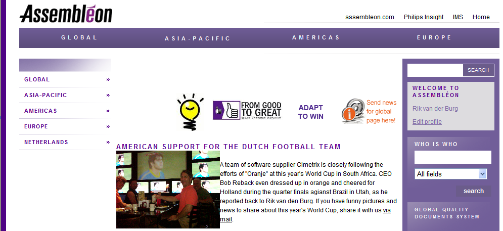
 and public speaker has been speaking and writing about the imperative need for American transition toward green energy for some time. His profound belief in superior American ingenuity and innovation, coupled with the rapidly growing world appetite for energy, is the potent recipe which should be directing our creative and practical energies toward a shift in US mentality that is not only good for our collective health, but also spells opportunity.
 I have been a Scoutmaster for the Boy Scouts of America for about 5 years now. Our troop goes camping several times a year. Utah offers a lot of beautiful and interesting camping areas. The variety is remarkable. In our troop we spent a lot of time teaching and preparing the boys to not only have fun, but also be safe and wise in their fun. Some planning ahead, training and common sense can make a huge difference. Nearly every week, I have our Senior Patrol Leader help all of the scouts in our troop recite a number of memorized phrases including the Scout Oath, Law, Slogan, Motto and sometimes even the Outdoor Code. The Scout Motto is the famous one known to almost everyone in the world; "Be Prepared". Reciting it every week helps our minds to remember to focus on being prepared for whatever may come. We prepare the boys to handle emergency situations such as medical and weather related emergencies. "Be Prepared" applies not only to scouting activities like camping, canoeing and hiking, but also to school, our careers and everything we do.


