Industry News, Trends and Technology, and Standards Updates

To the Cimetrix Community of Clients, Partners, Shareholders, and Employees

I believe that 2015 will be viewed as a significant turning point in the history of Cimetrix. When I accepted the role and responsibility of president and CEO of Cimetrix in 2001, Cimetrix was a publicly traded company. In addition to the normal challenges of running a business, Cimetrix was required to comply with all SEC reporting obligations. When the Sarbanes-Oxley Act (SOX) imposed additional financial reporting obligations with increased internal controls, Cimetrix was required to spend even more time and money. I’ve always believed if you are going to do something, you should do it to the best of your abilities. Consequently, Cimetrix dutifully fulfilled its quarterly SEC reporting and SOX compliance obligations. Every year independent SOX auditors performed the required annual audit and their reports always concluded that there were no material weaknesses in our financial reporting or internal controls.

IMG_5110-1For a small company like Cimetrix, we can be proud of these accomplishments. We are very thankful to have had Jodi Juretich as CFO for these past eight years. Jodi managed the company’s financials and was responsible for preparing all of our SEC filings. For those of you not aware, the SOX laws include significant personal liability for the CEO and CFO in the event of any material errors or misstatements. As a result, while we had no idea how many people might read our SEC filings (other than the fact that we know our competitors all meticulously read each and every one), each filing had to be reviewed not only internally, but also by SOX compliance consultants, auditors, lawyers, and the board of directors. Significant management time and precious time with our board of directors was spent reviewing and approving SEC filings. As I hope everyone can appreciate, this represented a huge burden for a small company like Cimetrix. In addition to the hard costs that we estimated at approximately $250,000 per year, it is difficult to overstate the amount of energy in terms of management time and attention that went into reviewing and approving not only the financial statements, but the mandatory narratives for these quarterly SEC filings.

Since the introduction of SOX, many public companies have made the decision to go private, and we received a lot of advice over the years that Cimetrix would likewise be much better off as a private company. As you can imagine, however, there are many factors that go into such a decision. We always considered what is best for our shareholders, clients, and employees. Accordingly we were careful and patient in waiting for the right opportunity. From our perspective, that opportunity arose last year, which allowed us to go private without the need for external capital or any dilution to our shareholders. We believe it was an excellent use of the company’s cash to remove the ongoing “tax” of being a public company, which we accomplished in late 2014.

As I reflect back on our first year as a private company, there were a number of highlights in 2015.

  • The change in management focus has been remarkable. From the board-level to the daily and weekly operational meetings, the focus is now centered on clients, products, and strategy. How can we better serve our clients? How can we operate more effectively and efficiently?

  • Maybe the timing was coincidental, but Cimetrix also completed a major corporate organizational restructuring in early 2015. We involved ten of our key employees in an off-site workshop to map out the type of company we wanted to be going forward. Using an experienced coach and facilitator, we spent time reviewing and reaching agreement on “core” items including our shared vision and values, identification of our core customers, what is our promise to our clients, what is our long term “big hairy audacious goal,” and, equally important, what are the things we should stop doing. We identified the key functions of the company and the people with the best skills and experience to lead those functional areas. The result was a much flatter organization with opportunities for some of our most experienced engineers to assume more management responsibility. It was a very energizing and invigorating process that aligned the entire company on the path forward.

  • We also made the commitment to go through our product lines and address all outstanding issues. Over time, the number of product issues that were not urgent or high priority had been slowly building. We made the decision that in order to position the company for faster long-term growth, as well as to reflect our values and brand promise to our clients, we should refresh our current product lines and drive the number of outstanding issues down to zero. This strategy will greatly reduce the long-term costs of maintaining our product lines going forward, as well as further improve the quality and performance of our industry leading product lines. It was wonderful to see the cooperation of our different departments work through the full database of all reported issues and reach resolution. During 2015 we completed new Service Releases for our GEM and GEM300 product lines, which included SECSConnect, CIMConnect, and CIM300, that resolved all reported issues and significantly increased the test coverage for each product. Our Product Management group coordinated the effort to resolve all issues with appropriate stakeholders. Once the backlog of work was clearly identified, our Software Engineering group accepted the challenge and took great pride in doing the work they had wanted to do, but never had had the time, to improve our products and significantly increase the level of automated tests.

  • As part of the strategy to improve our customers’ experience using Cimetrix products, we expanded our customer support group into a “Client Training & Support” group with an enhanced staff of senior engineers. Their responsibility is to demonstrate Cimetrix products during the sales cycle, train new clients, and serve as proactive technical liaisons as our clients progress through the critical development cycle. Initial feedback from clients has been outstanding. In particular, I had one new client tell me that in his experience, it is natural for the level of support to fall off a bit after they place an order for a product. However, in the case of Cimetrix, we provided a very high level of attention and support during the sales cycle, and once they placed the PO, they were pleasantly surprised to see that the level of attention and support from Cimetrix actually increased. While they have had problems with other suppliers “over-promising and under-delivering,” their experience with Cimetrix has been overwhelmingly positive, as our software does what we say it will do, and we provide very responsive and passionate support with senior engineering staff.

  • We have been at the forefront of the new industry standards for “Interface A,” or its alias “Equipment Data Acquisition (EDA),” for over ten years. When these standards were initially conceived and driven by representatives from Intel and AMD, we thought these new standards made logical sense and would ultimately be adopted by the industry, but we had no idea how long it might take for these standards to be adopted. A large semiconductor foundry in the industry has become the leading user of EDA. Our strategy has been to work closely with this company and the large number of equipment makers that selected Cimetrix’ CIMPortal Plus product to meet the company’s requirements for EDA. While Cimetrix did this facilitation work on our own dime, we believe this investment has paid off handsomely as we’ve helped many of our clients achieve good success in this company's factories, and, as a result, we now have very appreciative clients all over the world that serve as solid references for Cimetrix and our EDA products. In parallel, our Sales and Account Management team has been evangelizing the benefits of EDA to other semiconductor manufacturers. The list of companies now implementing some aspect of EDA has grown to include industry leaders such as Globalfoundaries, Infineon, Inotera, Samsung, Toshiba, and TSMC. The biggest news was Samsung announcing plans for an EDA pilot project in 2016. In a recent briefing to local Korea-based equipment makers, it was reported that some large equipment makers such as Applied Materials and Tokyo Electron developed their EDA solutions in-house, but “most of the rest use Cimetrix products.” To respond to these opportunities, the Cimetrix Sales and Account Management group worked quickly to establish relationships, distribution channels, and local sales and support for Cimetrix products in Taiwan and Korea. While Cimetrix has great partners in Japan, we have learned that each country is different and customers prefer to receive support from companies within their own country, in their native language. Dave Faulkner and Alan Weber logged many miles this year explaining the best practices for EDA and establishing these very important relationships for Cimetrix, which we believe position Cimetrix to sell and support our products more effectively within these markets. In 2016 Cimetrix is scheduled to exhibit in industry trade shows in Korea, China, Taiwan, and Japan that we believe will lead to new clients in these growing markets.

  • Lastly, even though we are no longer required to publish SEC filings, we maintain the same high level of internal controls and fiscal discipline. The only difference is we don’t go through the seemingly endless quarterly reviews and narratives. The semiconductor capital equipment market is widely reported to have declined during 2015 and is expected to be flat for 2016. Cimetrix has noticed similar trends among our client base. During 2014, Cimetrix was profitable every quarter with total revenue in the $6 to 7M range with over $500,000 of adjusted EBITDA. For 2015, we continue to operate profitably on a quarterly basis and expect to have similar full-year financial results as 2014. We expect to end the year with close to $2M of cash and, of course, no debt.

Going Forward

Going forward, industry analysts predict a decrease in semiconductor capital equipment spending for 2016. Cimetrix has a number of irons in the fire that we hope will counteract the overall industry trends and enable us to grow next year. We have some major clients in adjacent markets that have the potential to contribute increased revenue. We also hope to get some traction from our efforts to add new clients and grow revenue in the Taiwanese, Korean, and Chinese markets. However, as we have learned over the years, it takes time to develop such new markets, so we are not planning to see large increases in revenue in the immediate future.

Japan show

By working closely with our clients in semiconductor and adjacent markets, we have identified a number of opportunities for new products. We plan to continue to invest in our current product lines for GEM, EDA, and Equipment Control, as well as look for opportunities to develop new products in conjunction with industry leaders.

If I sound excited about the future for Cimetrix, it is because I am. We have a great team here at Cimetrix and we added a number of solid new team members during 2015. While we have made great progress, we are never satisfied, and will strive for continual improvement as we pursue closer relationships with our clients, improvements in our efficiency and effectiveness, and above all, building great products that help our clients be successful and perform well for those they care about.

I want to thank our clients for the faith and confidence they have placed in Cimetrix’ products and team members, our employees for their passion, dedication and commitment, and our shareholders for their patience that we believe will ultimately be rewarded.

Topics: Semiconductor Industry, EDA/Interface A, Customer Support, Doing Business with Cimetrix, Cimetrix Company Culture, Investor News

SEMICON Japan 2015 Spotlights IoT and its Effects on the Semiconductor Industry of the Future

December 16-18 in Tokyo, SEMI played host to SEMICON Japan that was co-located with the WORLD OF IOT, a special “show-within-a-show” dedicated to the Internet of Things usages that are propelling the next generation of microelectronic advances. SEMICON Japan is of note as Japan has the world’s largest installed fab capacity with more than 4.1 million 200mm equivalent wafers per month representing a high product mix.

Over 60,000 visitors attended the three-day event who met with nearly 800 exhibitors; attended forums, technical sessions, and networking events; and had the opportunity to see new innovations and technologies within the industry.

semicon japan.jpg

Semicon Japan

Semicon Japan

One highlight of the show was the Sustainable Manufacturing Pavilion. The pavilion focused on 200mm fab capacity where increased demand from IoT devices is anticipated. Revamping of the existing capacity and building cost-conscious capacity will be key to the sustainable growth of the industry. Sustainability in microelectronics manufacturing is quickly moving from a minor area of focus to a major consideration in business planning. Forward-thinking device makers, materials suppliers, and equipment manufacturers are all beginning to understand sustainable manufacturing makes economic sense for the future.

The pavilion offered many related sessions throughout SEMICON including the SEMI Technology Symposium Test Technologies for Automotive Semiconductors; the SEMI Technology Symposium on DFM in the Trends towards Fabless/Foundry Manufacturing and Alliances; the SEMI Technology Symposium on The Dreams and Reality of TSV/2.5D/3D Packaging; and a Sustainable Manufacturing and High Tech Facility Forum.

This year’s SEMICON Japan also featured a Manufacturing Innovation Pavilion that showcased inventive processes, equipment, manufacturing, components, and materials technologies that enable smarter and faster—yet cheaper—semiconductor devices to create our advancing society, industry, and life. The pavilion demonstrated that developing microelectronics technologies that will make the IoT possible requires continued innovation in semiconductor manufacturing equipment, materials, and components.

In conjunction with the Manufacturing Innovation Pavilion, SEMICON conducted a Semiconductor Executive Forum, a Lithography Business Forum, and a Manufacturing Innovation Forum to exchange ideas and share knowledge about the topics featured in the pavilion.

The WORLD OF IOT brought together leading global electronics and microelectronics companies whose innovations are driving the expansion of mobile technologies, cloud computing, and network-connected devices. Held in conjunction with SEMICON Japan, WORLD OF IOT was a "show-within-a-show". Exhibitors included such noteworthy companies as Tesla Motors, Toyota Motor Corporation, and Intel KK that demonstrated current projects and developing technologies. Executive forums and technical sessions were also offered everyday during the show.

Cimetrix was proud to be represented by our two distributors in Japan, Meidensha Corporation and Rorze Corporation, who both featured our SECS/GEM and EDA product lines. For Rorze, 2015 has been a significant year, the company celebrated its 30th anniversary. Stay tuned for my upcoming blog about its amazing anniversary celebration.

SEMICON Japan 2015 made a great end cap to the year as it focused so heavily on where the semiconductor industry is headed. Hopefully all the SEMICONs in 2016 will continue to be forward-looking as we here at Cimetrix are and remain focused on seeing how managing big data is becoming an ever more important issue within manufacturing. For more information on how EDA/Interface A is equipped to manage data acquisition in fabs, click here.

Topics: Semiconductor Industry, EDA/Interface A, Partners, Events, Data Collection/Management

Manufacturing Applications for Leveraging a Factory-wide EDA Implementation

Posted by Alan Weber: Vice President, New Product Innovations on Dec 16, 2015 8:52:49 PM

In our November EDA-related blog, I covered highlights of the Factory System Infrastructure topic shown in the figure below, and emphasized the need to have a long-term architectural vision to guide the development of a scalable data collection and management environment. Today’s topic completes the picture by summarizing the kind of Manufacturing Applications that can leverage a factory-wide EDA implementation. Unlike infrastructure software alone, these applications are what really provide the ROI for the process engineers and other factory customers of the manufacturing IT department’s efforts, so it is important to understand the scope and requirements of these key applications early in the strategic planning process.

Automation_Strategy_Framework_Mfg_Apps.jpg

Even though Cimetrix is principally in the business of providing software products that enable equipment suppliers to provide data using EDA technology to the factory application developers that use the information in their production systems, we’ve been involved in this process for many years, and have a good idea of the dominant uses of this data to improve manufacturing Key Performance Indicators (KPIs). So in this blog, I’ll cover a little of the high-level picture of what applications fully leverage EDA data.

First and foremost, it is very easy to connect a basic EDA client to a piece of equipment, upload its metadata, and collect information about that tool’s behavior, so implementing a generic “quick-connect production monitor” independent from the fab-wide data collection system is a very common use for EDA. Moreover, if the model in the tool is compliant to the E164 (EDA Common Metadata) standard, you can make a lot of assumptions about the names of the modules, the wafers, the substrate locations, the process jobs, etc., since all of this information is standardized. As a result, you can quickly get an idea of what the equipment is doing, what recipes it is running, what wafers are being processed, and how well the tool is performing with no custom software whatsoever.

Once this is accomplished, the next step most process and equipment engineers take is to more fully characterize the tool’s behavior, so a very common use of EDA is simply improving equipment and process visibility. By inspecting the equipment model, you can see all the events and parameters that are available to be collected, plot them in Excel or on real-time strip charts, or pass them to other analysis applications.

After the equipment has been characterized, the first major production application most fabs will implement is multivariate fault detection (MVA FDC). This is actually the predominant application of EDA data in the industry to date, because in order to do well-architected fault detection applications, one must “frame” the trace data very carefully. High-speed data collection is usually only required in a small number of specific recipe steps after certain conditions have been established, so you can use EDA’s powerful event-based trace data collection to frame the precise data you want, and pass that on to the multivariate control and fault models.

Of course, once you understand a tool’s behavior and have good fault detection capability, you then start to use EDA data to compare tools across a fleet. You would normally want a set of similar equipment to behave in the same way, but perhaps you have one tool that performs exceptionally well, and you’re not quite sure why…In this case, you do what’s called a “golden run” analysis on that equipment, and compare the key trace variables in one with like variables in similar equipment to see where the differences are, and try to explain why those differences exist. Other names for this class of applications include chamber matching and tool matching.

Another key application that we’re starting to see significant interest in is external sensor integration. Factories are now starting to use EDA to present information collected from independent sensors alongside the information collected directly from the equipment. Sharing a common equipment model across these systems effectively “unifies” that data, so the downstream analysis applications believe the information was collected from a single, integrated source. The EDA metadata model offers an ideal way to accomplish this unification.  

Finally, in many advanced wafer fabs, it is important that substrates do not “sit around” after they’ve been processed. Minimizing inter-process wait times is especially important for some advanced processes, so knowing a priori—the precise moment that a lot is going to complete—is a critical capability so the material handling systems can be scheduled to pick up that material and take it to the next process. EDA provides an ideal way to make these predictions generically for multiple process types using the information that is required in the equipment model.

We’ll address these last two applications—external sensor integration and lot completion estimation—in more detail in later blog postings, but I wanted to get you thinking about these ideas early in the discussion of real EDA usage in semiconductor factories.

There are many more EDA application ideas and examples we could share at this point, from component fingerprinting to wait-time waste analysis to dynamic sampling for wafer-level feedback control to feature extraction for predictive maintenance…but these just scratch the surface of what factory customers will come up with once they experience firsthand the flexibility and power of EDA in their factories. More later as this creative process unfolds!

To schedule a time to discuss your EDA needs, click here to set-up a time to talk with one of our knowledgable experts.

Topics: Industry Highlights, EDA/Interface A, Doing Business with Cimetrix

Factory System Infrastructure Support Necessary for a Full-scale EDA Deployment

Posted by Alan Weber: Vice President, New Product Innovations on Nov 24, 2015 12:30:00 PM

In my October 27th blog, I wrote about the Equipment Automation topic shown in the figure below and stressed the importance of developing good equipment purchasing specifications from the outset to ensure the company’s manufacturing objectives can be met. Given the number of EDA pilot and production projects currently active across the industry, it’s likewise important to consider what kind of Factory System Infrastructure will be necessary to support a full-scale EDA deployment… so the purpose of this posting is to highlight this topic for the semiconductor manufacturing IT professionals who may face these challenges soon.

Automation strategy frameworkHowever, before diving into a detailed design process for an EDA factory system, you must decide what overall system architecture will govern that design. A number of factors go into this decision, including 1) the functional requirements that distinguish EDA-based data collection from other more traditional approaches, 2) technology constraints of the existing factory systems, 3) budget limitations, 4) schedule requirements, and especially 5) the non-functional requirements (scalability, performance, reliability, ease-of-use, etc.) that often make the difference between success and failure of a given system.

Each of these factors deserves a thorough treatment of its own, but since we were invited to address this topic at a recent seminar sponsored by SEMI Taiwan, we’ve assembled an overview presentation entitled “Factory Systems Architectures for EDA” that you can use as a starting point. It not only covers in more depth the requirements above which drive key architectural decisions, but also suggests what some of the major architectural components of a production system would need to be, based on the experience Cimetrix has gained working with the earliest adopters of EDA across the semiconductor device maker and equipment supplier communities. These include provisions for handling the scores of equipment metadata models that will exist in a production facility, for creating and managing the thousands of data collection plans that are resident at the equipment instances themselves, for monitoring and maintaining the overall performance of a system with such inherent flexibility, and for a number of other examples. Finally, the presentation describes some high-level examples of architectural “styles” that have been implemented in the industry thus far.  

We sincerely hope you will download this presentation and its companion “The Power of E164: EDA Common Metadata” that was also presented at the SEMI Taiwan event, and contact us when you want to know more about any of these topics.

Topics: Industry Highlights, EDA/Interface A, Doing Business with Cimetrix, Data Collection/Management

To Better Serve Our Clients, We Will Be Discontinuing the Mailing of CDs and Hardcopy COAs for Runtime Licenses

We here at Cimetrix are excited that we are implementing a new process that will both benefit our clients and the environment. We have always delivered our software runtime license orders to our clients on CDs along with hardcopies of their Certificates of Authenticity (COA). Well, starting January 1st, we will begin delivering orders to our clients through emails that will include a digital COA for each runtime license and instructions on how to download their software.

As a company, we have always prided our self on providing the finest quality customer experience possible so we feel that this new process is just one more step in improving our service. There are a number of benefits of this change:

  • Most of our clients integrate Cimetrix’s software with their own software by using the Software Development Kit (SDK), most runtime license CDs are simply thrown away, which in today’s world is really not acceptable. By making this simple change, we will be eliminating thousands of pounds of potential waste.

  • We are constantly improving our software products and the latest version should always be obtained from our Support website (cimetrix.com/online-support)—not from a CD stored on a shelf somewhere for who knows how long. This change ensures that the latest version of our software will always be used.

  • The shipping cost and time delay by sending CDs by a carrier will be eliminated which will be a direct cost savings to you. 

  • The proof-of-purchase for our runtime license is the COA, not the CD. The COA number is what is used to obtain the license code using our online license generator. 

So the only thing we need our clients to do is to make sure we have an email address on file of where they would like their future orders sent. It’s that simple. We do foresee a period of adjustment for some clients, so for those that still want CDs and hardcopy COAs delivered, we will have this option available for an additional fee.

Of course, if you have any questions or comments regarding this policy, we are always happy to hear from you.  You can contact us at Orders@Cimetrix.com.

Topics: Customer Support, Doing Business with Cimetrix, Cimetrix Products

Creating Good EDA Purchasing Specifications

Posted by Alan Weber: Vice President, New Product Innovations on Oct 27, 2015 1:00:00 PM

The past few months have been full of news regarding adoption of the SEMI EDA (Equipment Data Acquisition, or Interface A) suite of standards by a number of major semiconductor manufacturers, which has quickly rippled throughout the supplier community as equipment makers and software providers alike consider the implications for their product road maps and support teams.

The range of EDA-related projects now underway covers the full spectrum from basic experimentation with this new data collection paradigm on a couple of tools to integration of these data sources with factory-level predictive analytics platforms to full factory pilot deployments. And although the specific requirements for the equipment suppliers involved in these projects may seem to be very different at the outset, eventually the fab purchasing departments will set a target for EDA interface functionality and performance that is high enough to support their automation requirements for the next 5-7 years.

What this means in practice is that even though the current specifications may be fairly loose regarding which “Freeze” level (I or II) is called for and what the equipment metadata model structure and content should be, eventually the factory customers will fully understand the benefits they can achieve by requiring the latest versions of the entire EDA suite (especially the E164 Common Equipment Metadata standard), and will revise their specifications accordingly. For this reason, it makes perfect sense for equipment suppliers to plan for this level of implementation now rather than waiting for it to be required across the board. This is especially true for suppliers who are just beginning their EDA implementations, as it is no more difficult to build a Freeze II-/E164-compliant interface using today’s EDA development software products than a less capable interface.

From the factory customer usage perspective, it is important to consider the distinguishing features of the EDA standards when developing new purchasing specifications. In particular, unlike SECS/GEM, much of the EDA interface capability is dictated by the structure and content of the equipment metadata model, so this must be carefully designed to ensure that the automation requirements and performance expectations are clearly communicated. This may in turn require more direct involvement of the process, equipment, and industrial engineering teams than ever before.

Automation Strategy frameworkMoreover, when communicating these requirements to the OEM community, it is useful to explain what strategic manufacturing objectives are being addressed and what the information will be used for; this context helps the suppliers understand why the specs may include a high level of detailed information, and can shift a potentially adversarial negotiation process more towards a teaming relationship based on shared objectives.

Fortunately, Cimetrix has many years of experience not only working in the EDA standards development process, but also providing products and services to the early fab adopters of this technology and most of their equipment suppliers. As a result, we have developed a pro forma set of EDA implementation guidelines which can easily be adapted to a specific factory’s purchasing requirements, and are happy to work with you to evaluate your needs and apply this process.  

For more information about developing good EDA purchasing specifications, check out the video we’ve prepared at the link below – and then let us how we can help!

Watch the Creating Good EDA   Purchasing Specifications Video

Topics: Semiconductor Industry, EDA/Interface A

2015 Advanced Process Control (APC) Conference Focused on High Quality Equipment Data

Posted by Alan Weber: Vice President, New Product Innovations on Oct 23, 2015 1:00:00 PM

01_Flags_above_Austin.jpg

02_APC_Conference_Banner.jpg

03_Jalepenos.jpg

04_APC_Conference_Agenda_Cover.jpg

Cimetrix participated in the recent Advanced Process Control (APC) Conference in Austin, Texas, along with more than 120 control professionals across the semiconductor manufacturing industry. This conference, now in its 27th year, is one of only a few global events dedicated to the domain of semiconductor process control and directly supporting technologies, so it was encouraging to see its attendance and energy level rebound from its low water mark a few years ago. The calendar may have indicated it was fall, but nobody told the weather forecasters… Austin set temperature records that week, even hitting 99°F one day!

Given the importance of high quality equipment data for all types of equipment- and factory-level process control applications, it is vital that Cimetrix and its customers understand the current requirements and future direction of this industry segment. Many presentations addressed these topics indirectly, but perhaps the newest insights in this regard came not from the wafer fabrication processes, but rather from the Back End, OSAT (Outsourced Assembly and Test), and advanced packaging segments.

As evidence, a number of presenters mentioned the growing need for equipment data collection in these areas, and cited the following reasons: 1) increasing demands by the consumer product manufacturing customers of these facilities (especially smart phone providers, but others as well) for equipment data to support their product quality and supply chain optimization initiatives; 2) emphasis on the Overall Equipment Effectiveness (OEE) productivity metrics, and the event/status data needed to support their automated calculation; 3) broader deployment of multi-variate Fault Detection and Classification (FDC) applications, which require more equipment trace data parameters than have typically been collected from back end equipment; and finally, 4) actual feedback control based on back end metrology – the best example of this presented last week was an application on dicing equipment that showed how kerf data collection and analysis can be used to adjust saw process parameters

The takeaway for Cimetrix in all this is that the back end equipment suppliers will need to anticipate this demand and may need to upgrade their interface capabilities substantially.

Since some of Cimetrix’ customers have pioneered the application of the latest generation of SEMI EDA (Equipment Data Acquisition) / Interface A standards in plumbing data from external “add-on” sensors to fault detection applications, I presented a generalization of this approach during one of technical sessions. This presentation, “Data Fusion at the Source: Standards and Technologies for Seamless Sensor Integration” is available on the Cimetrix website for those who want to learn more about how this is done.

05_Weber_Presentation_Cover.jpg       Download Presentation  

Check back next week to learn more about creating good EDA/Interface A purchasing specifications.

Topics: EDA/Interface A, Events, Data Collection/Management

SEMICON Europa 2015 Offers Insights into Upcoming Trends in the Semiconductor Industry in Europe

This week Cimetrix exhibited at SEMICON Europa 2015 along with about 400 other companies in the semiconductor industry in Dresden, Germany. The leading trade fair offered a chance for members of the industry to learn about new topics, information, and opportunities to help support and further develop the semiconductor industry across Europe.

An estimated 6,000 were in attendance at this SEMI-sponsored event. Some of the highlights of the three-day event were:

  • The Industry 4.0 Session: The term "Industry 4.0" has been established to describe the penetration of information science into manufacturing forming the next industrial revolution. The TechArena provided information about different aspects of this process.

  • The Emerging Research, Materials and Processes Session: The nanoelectronics research community is continuously exploring a range of new materials to enable further scaling of semiconductor devices and associated technologies, as well as many potential methods to create these materials with methods that allow utilization for future technology nodes. In this session several of these new materials and process developments were discussed by experts in their specific fields. Focus was on the unique properties of the materials or processes, what makes them specifically suitable for targeted applications, how they are characterized and/or how they can be fabricated. Among the topics that were presented were the newest developments for GaN processing, two-dimensional semiconductors devices and fabrication, metal organic frameworks as low-k materials, advanced memory materials such as FeRAM or MRAM Spintronics, and Selective Atomic Layer Deposition.

  • The Semiconductor Technology Conference (STC): This conference explored the efforts of our industry to ensure productivity enhancements for future advanced technology nodes, considering both a wafer size transition, and a continuation of current state of the art and smaller wafer sizes. Updates from around the world on wafer size transition activities were heard and there was a dedicated focus on “beam-based” metrology activities from METRO450 in Israel. SEMI invited their partners to share with attendees their insights, activities, and results in the preparation of future offerings of process equipment, materials, IT/fab automation systems, facilities and fab infrastructure, in order to rise to the challenge to ensure a continued economic manufacturing of state of the art semiconductor chips.

This year we exhibited as part of Silicon Saxony's Industrie 4.0 booth that consisted of about 40 kiosks representing companies with varying focuses within the industry. On Wednesday night, Silicon Saxony played host to all of the booth's exhibitors in a "Countries of Europe"-themed party. The event gave the Cimetrix team a chance to catch-up with friends and colleagues, and discuss new business opportunities. We'd like to thank Silicon Saxony for the great networking opportunity.

We are looking forward to SEMICON Europa 2016 in Grenoble, France next October and hope to see you there. If you didn't get a chance to meet with Cimetrix in Dresden this week and you would like to learn more about our complete line of factory connectivity and equipment control software solutions, please click here

Topics: Semiconductor Industry, Events, Smart Manufacturing/Industry 4.0

SEMI Standards Meetings from the North American Information & Control Committee Forecasts the Direction of the Semiconductor Industry

Posted by Brian Rubow: Director of Solutions Engineering on Sep 29, 2015 1:30:00 PM

During the week of SEMICON West in San Francisco this past July, the North American Information & Control Committee met to discuss and consider new and pending standards within the industry. SEMATECH was noticeably absent from the sessions. For many years, SEMATECH has been a leader in developing and promoting the GEM 300 and EDA standards.

Here are the highlights from those meetings and how they will effect you.

The DDA Task Force is in the early stages of planning a Freeze 3 version of the EDA (Interface A) standards. This may cause some concern—especially with OEMs—as some are just now getting their Freeze 1 interfaces accepted in Fabs. Freeze 2 was a big step forward in making the standards clearer and easier to adopt, but it required a lot of work to move from Freeze 1 to Freeze 2. The hope is that the transition from Freeze 2 to Freeze 3 will be easier, but there will be doubt and concern among many OEMs.

One of the changes proposed for Freeze 3 is replacing the usage of SSL (HTTP) with WS-Security, an extension to SOAP and a member of the web services specifications published by OASIS. This extension allows for secure data within a SOAP message, while still using HTTP for data transfer. This is really an underlying issue and should not affect the applications that would interface with our CIMPortal Plus product. It would allow for a secure connection between CIMPortal and the Fab client so that the data transmitted is protected from theft. There would be configuration changes required to allow the secure connection to be defined, but—once it is—the actual interaction between the OEM’s application and CIMPortal Plus should not change.

Another change being considered is the implementation of WS-ReliableMessaging, another extension to SOAP and also a member of the web services specifications published by OASIS. WS-ReliableMessaging describes a protocol that allows SOAP messages to be reliably delivered between distributed applications in the presence of software component, system, or network failures. Just as the WS-Security item above, this would be at the protocol level, an “under-the-hood” change. It should not affect the way applications interact with our product, but should provide for a more reliable connection to the host EDA client. Use of this extension could also allow EDA to be used in more factory applications, where guaranteed data acquisition is required.

The final issue that was discussed relating to Freeze 3 was a new high-frequency trace for collecting data at very high speeds triggered for short periods of time where the collected data is sent at the end of the collection period. For example, a 1 ms trace for 5 seconds where the 5,000 collected samples for each parameter would be sent at the end of the 5 second period. This change might require alterations in our products. This will help the data reporting be more efficient. Rather than reporting small individual pieces of data to the EDA client, this will allow many data samples to be sent together making for more efficient use of the network.

The GEM 300 Task Force had three ballots on hold due to the ongoing SML copyright legal trial between SEMI and The PEER Group. However, work on other pending ballots continued. The first, Ballot 5872, proposes to add new features to the E172 SEDD standard. E172 is a new standard that provides an XML schema for documenting a GEM/GEM 300 interface. Eventually, E172 can completely replace the current GEM documentation requirements.

Recipe Integrity ballot 5618 has an uncertain future since ISMI failed to pursue its development; unfortunately, the ballot had seemed very close to completion. This standard says that it will not require changes to SECS II messages, but simply clarifies what parameters are defined and how the existing pieces work together. So, essentially, it would be a standard that tells you how to use other existing standards.

Finally, the Task Force discussed enhancing the GEM 300 standards to handle equipment that bond substrates and divide substrates. This will affect E90 and could affect E40, E87, and E94 as well. These changes would likely require updates to CIM300. Right now the standards just address how to treat equipment where the same material (substrates or wafers) go in and out. Traditional material tracking assumes one wafer in, get processed, then return to an output carrier. In the proposed case, either two wafers go in and one unit comes out, or one substrate goes in and two come out

The committee is scheduled to next meet in November, so you can plan on seeing another post from me on the outcome of those meetings afterwards. Subscribe to our blog in the upper right corner of this page to be sure not to miss that or any of my future updates on the North American Information & Control Committee.

Topics: Industry Highlights, Semiconductor Industry, EDA/Interface A, Events

EDA Standards Seeing Increasing Adoption Across the Industry

Posted by Alan Weber: Vice President, New Product Innovations on Sep 22, 2015 9:19:21 PM

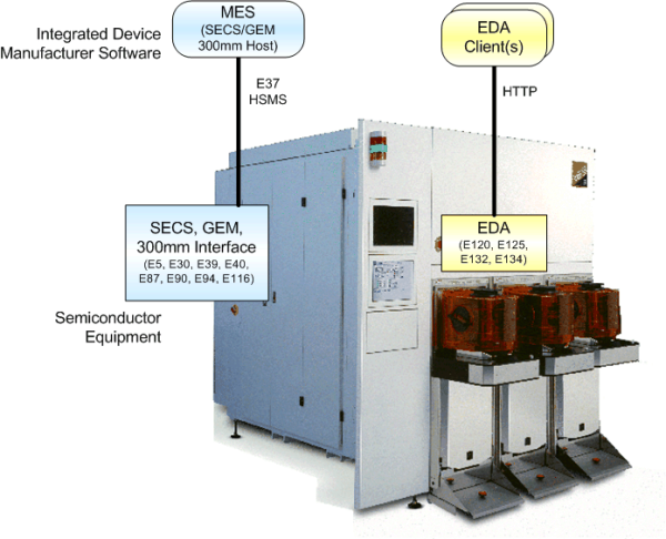
As mentioned briefly in a previous posting, the adoption momentum for the SEMI EDA (Equipment Data Acquisition) suite of standards has picked up noticeably over the past 6 months, and a number of pilot projects are now underway at leading chip makers across the industry, especially in Asia. As these projects bear fruit, we expect to see explicit requirements for EDA interface capability in the purchase specifications of many more fabs in the coming months. But that’s just a start.

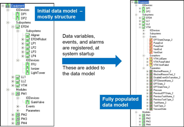
The early adopters of these standards who have now accumulated years of production experience clearly understand that the key to realizing the full manufacturing benefit of this technology lies in the structure and content of the equipment metadata models, which to date have been largely determined by the equipment suppliers themselves. The resulting diversity of EDA implementations is reminiscent of the situation that existed in the days before GEM, when every chip maker required their own particular “dialect” of SECS-II, and the equipment suppliers had to support a custom interface for each customer… not a pretty picture.

Luckily, the standards community recognized this problem early on, and addressed it via the Specification for EDA Common Metadata (SEMI E164). This standard effectively unifies the equipment models across the fab, regardless of process type or supplier, enabling the factory software developers to create generic manufacturing applications that “plug and play” with the equipment to address the problems that are common to all (status and productivity monitoring, material flow, resource utilization, etc.). 

EDA1.jpg

As a result, the next wave of factory implementations can directly leverage these lessons learned by requiring compliance to “Freeze 2, E164” level of the EDA standards suite, and focus their energies on new application development rather than supplier-specific custom integration software. Given the years of experience Cimetrix has dedicated both to the development of the EDA standards in the SEMI community and in providing product-based implementations on “both ends of the wire” (in other words, equipment and client/host side), we can support customers wherever they are in the implementation life cycle, from building awareness to initial purchase specification development to system architecture and application design to conformance and acceptance testing.

For more information about how we can help align your activities with this accelerating adoption process, please contact us… and stay tuned for more specifics on all the above!

For an introduction to EDA, download the presentation Interface A Overview: Characteristics, Benefits, and Applications.

Topics: Industry Highlights, Semiconductor Industry, EDA/Interface A