Industry News, Trends and Technology, and Standards Updates

Alan Weber: Vice President, New Product Innovations

Alan Weber is currently the Vice President, New Product Innovations for Cimetrix Incorporated. Previously he served on the Board of Directors for eight years before joining the company as a full-time employee in 2011. Alan has been a part of the semiconductor and manufacturing automation industries for over 40 years. He holds bachelor’s and master’s degrees in Electrical Engineering from Rice University.
Find me on:

Recent Posts

SEMICON Taiwan and eMDC: Join Cimetrix in Smart Manufacturing Events

Posted by Alan Weber: Vice President, New Product Innovations on Aug 24, 2017 11:15:00 AM

The week of September 11 will be a big one for Cimetrix in Taiwan. In addition to exhibiting at SEMICON Taiwan for the third year in a row (Booth # 2926) with our local partner, Flagship International, Cimetrix is privileged to be making joint technical presentations with GLOBALFOUNDRIES in two distinct events.

semitaiwan_banner.jpgFirst of all, Alan Weber (Cimetrix) and Mark Reath (Senior Member of Technical Staff, GLOBALFOUNDRIES) will share the stage at the Smart Manufacturing Forum at the Nangang Exhibition Center during the show on Wednesday afternoon (September 13, 12:40–1700, Room 402ab). Their presentation is titled “Smarter Manufacturing through Equipment Data-Driven Application Design” and highlights the importance of robust, standards-based data collection capabilities on both the equipment and factory sides in realizing the industry’s Smart Manufacturing objectives.


TSIA.png

On Friday of that week, this same duo will present “Device Scaling vs. Process Control Scaling: Advanced Sensorization Closes the Gap” at the Ambassador Hotel in Hsinchu on September 15, at 08:30–16:40 (click on the “Program” link). This presentation discusses how GLOBALFOUNDRIES is addressing the need for precise fault detection and process control in the sub-10nm domain  through integration of high-speed, process-specific sensors using its EDA (Equipment Data Acquisition standard) infrastructure to deal seamlessly with complex data types (e.g., spectral data) and the context information necessary to use this information effectively.  The conference agenda features speakers and topics across a broad spectrum of the industry’s value chain, so the conference promises to be an exciting and well-attended event.

In addition to these technical events, Cimetrix will be demonstrating its new EDATester™ product at the booth along with its complete family of connectivity and equipment control products.

We invite our customers and colleagues to join us at all of these venues and hope to see you in Taiwan soon.

Topics: Partners, Events, Global Services

Traceability Application Support: Episode 4 in the “Models in Smart Manufacturing” Series

Posted by Alan Weber: Vice President, New Product Innovations on Aug 1, 2017 11:15:00 AM

chicken_or_egg.jpg…never mind which came first… do you know where the chicken and the egg came from?

As integrated circuits increasingly find their way into applications for which human and environmental safety are paramount, the regulatory requirements related to product traceability become ever more stringent. For example, the automotive industry already requires that a device maker be able to provide a full manufacturing process history within 48 hours of a request for certain kinds of products, but this only scratches the surface of what’s to come in the growing markets for autonomous vehicles and their supporting public infrastructure, aircraft components, medical implants and diagnostic systems, and the like.

semiconductor_manufacturingThe good news in all this is that the latest semiconductor manufacturing equipment interface standards include enough information about the product being built and the processes used at each step along the way to directly support these traceability requirements with little or no custom software. Specifically, the SEMI Equipment Data Acquisition (EDA) suite of standards (also known as “Interface A”) defines the components of an explicit equipment model that can represent this information, and the SEMI E164 (EDA Common Metadata) standard goes so far as to specify the actual structure and naming conventions for the required components.

Before getting deeper into the specifics, let’s step back and define “traceability” in this context. According to ISO 9000 (Quality management systems – Fundamentals and vocabulary), the term means “the ability to trace the history, application or location of an entity by means of recorded identifications.” 

In a wafer fabrication facility, this definition covers a broad range of capabilities. The most basic interpretation could be satisfied by simply having an ordered list of the manufacturing equipment visited by each wafer (substrate) during its 3-month journey through the fab. As long as the manufacturer keeps a record of which substrate each assembled die came from (which most do), the required documentation could be generated from information contained in the MES (Manufacturing Execution System) and its associated scheduling/dispatching system. 

Symptoms_Problems_Cause_tree

However, at the other end of the spectrum, the traceability requirement may include not only the list of equipment visited, but also the recipe used at each equipment, the precise timing of wafer movement and process modules visited within the equipment, values of any adjustable recipe parameters and/or equipment constants that affect process behavior, batch identification and status information for any consumables used during the process, usage counts for any fixtures involved, operator interactions (if any), and so on. The reason for this level of detail is to enable the failure analysis engineers to identify the potential root causes for any field failures, and then determine what other devices in the field may be susceptible to similar failure conditions for product recall purposes.

To be sure, much of this information could be assembled after-the-fact from the various data bases maintained by the equipment and process engineering and yield management systems present in most modern wafer fabs, but this process can be complex, time-consuming, and error-prone. A better approach would be to generate the most commonly needed traceability records on-the-fly directly from information available in the equipment... and this is where the newest EDA standards enter the picture. 

By analogy, let’s look at an intuitive example: a commercial cake baking enterprise. Even for a relatively simple (compared to semiconductor manufacturing) production process, full traceability requires information from the raw materials suppliers through the manufacturing process to packaging and finished goods warehousing. You can see in the picture below that material, recipe, and equipment setup information is included in the records produced.

Complete Production Traceability

In a unit of semiconductor manufacturing equipment with an E164-compliant interface, these types of information appear in various sections of the equipment metadata model. Specifically, material-related information is captured in the “Material Manager” logical component, shown in expanded view below* to highlight the state transition events and parameter data available for each substrate during its transportation and processing in the equipment.

Material_Manager_component

Recipe-related information is found in the physical modules responsible for substrate processing (“ProcessingChamber1” and “ProcessingChamber2” in the example below), within the “E157-0710:ModuleProcess” state machine, dictated by the SEMI E157 (Module Process Tracking) standard and required by E164. Note the rich list of context information available at every recipe step, including the RecipeParameters array, in the expanded model excerpt below. RecipeParameters_arrayTaken together, the timing and parameter data from these two sections of the equipment model supply most of the information required for full wafer fab traceability. Moreover, since SEMI E164 actually standardizes the event and parameter names in the model, the DCPs (data collection plans) that collect this information can be programmatically generated and activated for all the equipment that is E164-compliant. This represents a significant engineering cost reduction over the conventional methods used to identify, collect, and manage this information. The figure below is one visualization of such a DCP.DCP_Visualization

When extended beyond individual devices to circuit boards, modules, and completed parts (see the example below for an automobile speedometer), these requirements require even more bookkeeping… but that’s a topic for another day!automobile_speedometer

This article is the fourth in the series recently announced in the Models in Smart Manufacturing Series - Introduction, be sure to watch for subsequent postings that will expand on this theme. 

We look forward to your feedback and to sharing the Smart Manufacturing journey with you.


*The visualizations of equipment metadata model fragments and DCP contents are those produced by the Cimetrix ECCE Plus product (EDA Client Connection Emulator).

Topics: EDA/Interface A, Models in Smart Manufacturing series, Smart Manufacturing/Industry 4.0

Precision Data Framing during Process Execution – Tricks of the Trade: Episode 3 in the “Models in Smart Manufacturing” Series

Posted by Alan Weber: Vice President, New Product Innovations on Jun 27, 2017 11:30:00 AM

…or how to move away from “just in case” data collection...

It’s a common process engineering request of the manufacturing IT folks: “Please collect as much data as you can during this process, and we’ll figure out what’s important later.” And this approach has worked fairly well up to this point. However, with 10nm (and below) production on the horizon, coupled with the desire to sample key parameters at ever-increasing rates, the amount of on-line data storage required to support this approach could skyrocket… to say nothing of the difficulty in sifting through all that data to extract the real information you wanted in the first place.

Models3.1.jpgModels3.2.jpg

Fortunately, you don’t have to look very far into the SEMI EDA (Equipment Data Acquisition) standards (also known as “Interface A”) to find an excellent solution alternative. The portion of the standard equipment metadata model (specified by SEMI E164 – EDA Common Metadata) that deals with process execution (SEMI E157 – Process Execution Tracking) combined with the conditional triggering features of Trace Requests (SEMI E134 – Data Collection Management) enables a process engineer to precisely collect the right data at the right time at the right frequency without over-burdening the equipment or factory systems by collecting and storing less important data at the highest rates. 

Let’s look at an example. The key state machine called for in the E157 standard (see figure below*) has 2 major states (NOT EXECUTING and EXECUTING) with intuitive transition events defined between them (Execution Started, Execution Completed, and Execution Failed). If you only care about tracking the overall execution time of the process recipes on a given tool, then a single DCP (Data Collection Plan) with a pair of Event Requests on the Started and Completed events is all you need. The difference in the timestamps of the corresponding Event Reports provides the necessary information. 

Models3.3.png

However, if you want to monitor a baseline set of equipment performance parameters at a low frequency (say, 1 Hz) throughout the recipe, and collect the key parameters for analyzing process behavior at a higher frequency (50 Hz) during the most critical process steps (5 through 8), you would use a DCP with multiple Trace Requests triggered by the Step Started and Step Completed transition events between the two sub-states (GENERAL EXECUTION and STEP ACTIVE) of the EXECUTING state. Furthermore, you would use the conditional triggering feature of the Freeze II version of the EDA standards (SEMI E134-0710 or later) to produce Trace Reports only during the critical process steps. The figure below is one visualization* of such a DCP.

Models3.4.png

You may have noticed from this example that multiple triggering conditions are ANDed together to determine whether or not to collect the data and generate a Trace Report. But how do you handle the situation in which OR functionality is needed to produce the desired result, for example, in the case that multiple sets of recipe steps are considered critical (say, steps 5-8 and steps 11-13)?

This is where you can use one of the “tricks of the trade.” Simply define multiple Trace Requests with different sets of ANDed conditions to cover the range of ORed situations. For the case above, you would need two Trace Requests: one for each critical set of contiguous recipe steps (see visualization below).

Models3.5.png

Note finally that you can also apply comparison operators to analog values to trigger Trace Requests, which may be especially useful to sample specific parameters when some value crosses an important threshold. 

Models3.6.png

Taken together, these techniques are sometimes called “data framing,” which is an important tool in the controlling the scope of factory data explosion that will soon be upon us. 

This article is the third in our Models in Smart Manufacturing series – be sure to watch for subsequent postings that will expand on this theme.

We look forward to your feedback and to sharing the Smart Manufacturing journey with you.

*The visualizations of equipment metadata model fragments and DCP contents are those produced by the Cimetrix ECCE Plus product (EDA Client Connection Emulator).


Topics: EDA/Interface A, Models in Smart Manufacturing series, Smart Manufacturing/Industry 4.0

European Advanced Process Control and Manufacturing Conference XVII: Retrospective and Invitation

Posted by Alan Weber: Vice President, New Product Innovations on May 17, 2017 11:30:00 AM

APC.jpgCimetrix participated in the recent European Advanced Process Control and Manufacturing (apc|m) Conference, along with over 150 control professionals across the European and global semiconductor manufacturing industry. The conference was held in Dublin, a lively city on the east coast of Ireland which features a charming juxtaposition of old and new and is home to 1.2 million of the friendliest and most talkative people on the planet! 

APC_2017_1.jpg

Of course, one of Ireland’s greatest “natural resources” may also contribute to their fine spirits…

APC_2017_2.jpg

This conference, now in its 17th year and organized by Silicon Saxony, is one of only a few global events dedicated to the domain of semiconductor process control and directly supporting technologies. This year’s attendance was up from that of the three previous years, a clear indication that this area continues to hold keen interest for the European high-tech manufacturing community. Moreover, the participants represented all links in the semiconductor manufacturing value chain, from universities and research institutes to component, subsystem, and equipment suppliers to software product and services providers to semiconductor IDMs and foundries across a wide spectrum of device types to industry trade organizations – something for everyone.

APC_2017_3-1.jpg

The local sponsor for the conference was Intel, which is the largest private-sector investor in the Irish economy and one of its biggest employers. In addition to excellent logistics support, Intel hosted a lovely evening of fine food and local entertainment at the world-renowned Trinity College.

APC_2017_4.1.pngAPC_2017_5.png

As in many prior years, Cimetrix was privileged to present at this conference. Alan Weber delivered a talk entitled “Smarter Manufacturing with SEMI Standards: Practical Approaches for Plug-and-Play Application Integration.” This topic was well aligned with one of the key themes of this year’s event, but stressed the point that our industry already has at its disposal many of the tools, techniques, and enabling standards required for Smart Manufacturing. Specifically, the presentation illustrated how the new SEMI E172 SECS Equipment Data Dictionary (SEDD) standard could be used to document an equipment’s GEM interface in way that provided much of the same hierarchical structure and context information inherent in the latest generation of EDA metadata models (SEMI E120, E125, and E164). If you want to know more, feel free to download a copy of the entire presentation from our web site.

In addition to Smart Manufacturing, recurring themes of the presentations included:

  • The IoT (Internet of Things) and interesting applications for all these “things” (e.g., most new drugs depend on a “smart delivery device” to be used safely and effectively)
  • Decision-driven data collection strategies (vs. “just in case” approaches)
  • Automated analysis, automated decision making, artificial intelligence, and other forms of machine learning
  • The evolution from reactive systems to predictive systems, or in Gartner’s terms, using data to move from hindsight to insight to foresight 
  • The increasing use eOCAP techniques (electronic aids and workflow engine support for Out-of-Control Action Plan execution) 
  • And, last but certainly not least, connectivity standards and technologies as key enablers of much of the above

The agenda also featured keynotes and invited talks from a variety of sources, namely:

  • Bosch – Success Factors for Semiconductor Manufacturing in High-Cost Locations
  • Intel – IoT’s Connected Devices and Big Data Analytics: the Opportunities and Challenges in Semiconductor Manufacturing
  • ST Microelectronics – FDC Control: the Loop Between Standardization and Innovation
  • IBM Research – Automating Analytics for Cognitive IoT 
  • Rudolph Technologies – Smart Manufacturing
  • Applied Materials – Advancements in FDC: Reducing False Alarms and Optimizing Model and Limits Management

The insights gained from these and the other 30+ presentations are too numerous to list here, but in aggregate, they provided an excellent reminder of how relevant semiconductor technology has become for our comfort, sustenance, safety, and overall quality of life. 

This conference and its sister conference in the US are excellent venues to understand what manufacturers do with all the data they collect, so if this topic piques your interest, be sure to put these events on your calendar in the future. In the meantime, if you have questions about any of the above, or want to know how equipment connectivity and control fit into the overall Smart Manufacturing landscape, please contact us!

Topics: Semiconductor Industry, EDA/Interface A, Events, Smart Manufacturing/Industry 4.0

Exposing Hidden Capacity through Material Tracking: Episode 2 in the “Models in Smart Manufacturing” Series

Posted by Alan Weber: Vice President, New Product Innovations on May 9, 2017 11:38:00 AM

“Do you know where your wafers are? Are you SURE?”

This adaptation of the famous public service announcement is as relevant for semiconductor process and industrial engineers as it was (and still is) for responsible parents. Given the ever-present productivity and profitability pressures in modern wafer fabs, it is essential to know the location and status of all product material at all times, because this information drives the scheduling and material delivery systems that provide competitive advantage for the world’s leading manufacturers. Until recently, material visibility at the lot/FOUP level was sufficient for this purpose, but this is no longer the case. 

Where_are_you.jpg

As production managers look for ways to squeeze more capacity out of their existing capital equipment, they realize that a deeper understanding of the wafer processing sequence within a particular tool type may provide opportunities to shorten the its overall lot processing time and increase the amount of material that can be processed simultaneously.  The first improvement results from identifying and eliminating unnecessary “wait” states* that individual wafers (or groups of wafers) may experience because of sub-optimal internal material handling, shared resource constraints, mis-calibrated subcomponents, poor recipe design, or a combination of these and other factors. The second improvement results from starting the next lot scheduled for a given tool as soon as all the wafers in the current lot have cleared the first stage of the process. This technique is sometimes called “cascading” or “continuous processing,” and applies to an increasing number of multi-chamber equipment types.

When applied to all the critical “bottleneck” tools in a factory, you can imagine what the resulting benefits would be for cycle time and capacity. Estimates of 3-5% improvement in these KPIs are not unrealistic.

Easy to say, right? But not so easy to implement? Perhaps not as daunting as you think…

The information required to track the precise location, movement, and status of individual wafers in semiconductor manufacturing equipment is most likely available for most equipment types in the form of “events” that chronicle the behavior of substrates, substrate locations, process chambers, aligners, wafer handling robots, and the other equipment components that affect wafer processing. What’s missing is a standard model that unifies this information across multiple equipment types, which would greatly simplify the data collection and analysis software required to implement a robust, generic material tracking system.

Here, too, the industry standards are actually ahead of today’s “state of the practice.” For example, the SEMI E90 “Substrate Management” and E157 “Specification for Module Process Tracking” standards define all the state machines, transition events, and associated context parameter data necessary to create a detailed Gantt chart of individual wafer movement and processing from start to finish, and allocate each contiguous time segment to its associated “active” or “wait” time element. The insights gained from this sort of visualization point directly to the opportunities cited above for improved tool control and factory scheduling.

Excerpts of these standards, a treeview representation of their respective models, and examples of the potential tracking displays are shown below.

Models_1.png

Models_2.pngModels_3.png

Models_4.png

Note that the SEMI E164 “Specification for EDA Common Metadata” calls for the inclusion of E90, E157, and a list of other GEM300 standards in the EDA equipment metadata model, so any E164-compliant equipment would directly and completely support such a material tracking application.

This article is only the second in the series recently announced in the Models in Smart Manufacturing Series Introduction posting – be sure to watch for subsequent postings that will expand on this theme.

We look forward to your feedback and to sharing the Smart Manufacturing journey with you.

*The list of potential “wait” states for semiconductor manufacturing has now been precisely defined and standardized as SEMI E168 “Specification for Product Time Measurement.” The standard also describes how they can be calculated using a specific set of standard material movement events commonly used in 300mm manufacturing equipment.

Topics: EDA/Interface A, Models in Smart Manufacturing series, Smart Manufacturing/Industry 4.0

Models in Smart Manufacturing Series – Introduction

Posted by Alan Weber: Vice President, New Product Innovations on Mar 24, 2017 11:30:00 AM

As a child I was an avid model builder—airplane models, trains, engines, cars, ships, even monsters (anyone remember “The Visible V8” and “The Creature”?)—anything I could get my hands on. At the time I didn’t reflect on the source of this fascination, but with the benefit of hindsight, it is clear that these models provided an interactive, tangible way to visualize, explore, understand, and enjoy the topics that were interesting to me. It was a way to enrich an otherwise intellectual activity.

Visible_V8.pngCreature.png

In fact, when Hurricane Carla ravaged the Texas coast and cut our electricity for 3 days, one of our luckier neighbors snaked an extension cord over the fence, which provided just enough power to run the refrigerator, a small black-and-white TV, and… you guessed it… my electric train. 

Model_train.png

More than four decades later, I still enjoy working with models, but in the high-tech manufacturing domain, they often operate in the reverse direction, providing a logical way to interact with and understand physical entities, like materials, fixtures, processes, devices, components, equipment, and entire systems. And as important as various model types have been throughout the relatively brief history of the semiconductor industry, they are increasingly an integral part of the “Smart Manufacturing” initiative that is sweeping a wide range of industries worldwide. 

The focus of my next few blog posts will be the specific models that are inherent in the communications interface definitions for manufacturing equipment, subsystems, and other devices that are expected to cooperate over the [Industrial] Internet of Things. Our first post in this domain almost a year ago introduced the notion that the metadata models called for in the latest generation of SEMI Equipment Data Acquisition (EDA) standards were already directly aligned with the Industry 4.0/Smart Manufacturing vision. This series goes into much more detail, showing how specific sections of the equipment models in the GEM and EDA standards directly support many of the factory monitoring, analysis and control applications that are essential for running a Smart Manufacturing enterprise (see Substrate Management example below).

substrate_management.png

Moreover, to the extent that the structure and content of these models can truly be standardized, their associated applications can be process- and supplier-independent, greatly reducing the development and support costs for the factory IT departments while providing useful capabilities for the production engineering and operations stakeholders.

To get a feel for the overall direction of this series, download the presentation "The Role of Models in Semiconductor Smart Manufacturing",  along with the transcript,  from the APC Conference held last October in Phoenix. Then watch for subsequent postings that address specific applications, from productivity (OEE) monitoring, material tracking, product traceability, process execution monitoring, and beyond.

We look forward to your feedback and to sharing the Smart Manufacturing journey with you.

Topics: Models in Smart Manufacturing series, Smart Manufacturing/Industry 4.0

EDA Testing – How is this accomplished today??

Posted by Alan Weber: Vice President, New Product Innovations on Feb 7, 2017 1:30:00 PM

Over the past several months, we have posted a number of blogs dealing with the testing of SEMI’s Equipment Data Acquisition (EDA / aka Interface A) standards suite. The first of these posts connected the importance of this topic to the increased adoption of the EDA standards across the industry, and broke the overall problem domain into its three major components. 

Subsequent postings provided additional detail in each of these areas:EDA_Icon.png

To bring this series to a close, this post addresses the “as-is” state of EDA testing as it is practiced today by the advanced semiconductor manufacturers who are requiring EDA interfaces on new equipment purchases and the suppliers who provide that equipment. 

For compliance testing, the three options in general use include: 

  1. ECCE Plus product- this software tool was originally developed under contract with the International Sematech Manufacturing Initiative (ISMI) to validate the fidelity, usability, and interoperability of early versions of the standard; it can used to manually execute a set of procedures documented in the “ISMI Equipment Data Acquisition (EDA) Evaluation Method for the July 2010 Standards Freeze Level: Version 1.0” document (see title page below) to exercise most of the capabilities called for in the standard; note that this is the only commercially available solution among the three.

ISMI.png

  1. Company-specific test suites – one major chip manufacturer (and early adopter of EDA) maintains its own partially-automated set of compliance tests, and provides this system to its equipment suppliers as a pre-shipment test vehicle. This set of tests is then used in the fab as part of the tool acceptance process; however, this system also includes a number of company-specific automation scenarios, which are not available for outside use. This highlights the need to support custom extensions in an industry-validated tester if it is to be commercially viable.

  2. In-house custom test clients – this is a variation of #2 that some of the major OEMs have chosen as their economies of scale dictate; the problems with this approach are that a) the test clients must be kept current with the EDA standards, which are themselves a moving target, and b) unless thoroughly validated by the eventual customers of the equipment, there is no guarantee that passing these tests will satisfy the final acceptance criteria for a given factory. 

For performance and stability testing, there are no automated solutions currently available. The ISMI EDA Evaluation Method does describe some rudimentary performance evaluation procedures, but these no longer reflect the expectations of the customers with many years of accumulated EDA production experience. Clearly a better solution is needed.

Finally, for metadata model conformance testing, the only available solution is the Metadata Conformance Analyzer (MCA) that was commissioned by Sematech and implemented by NIST (National Institute of Standards and Technology). It has not been updated in almost five years, and exhibits a number of known issues when applied to a SEMI E164-compliant equipment model (E164 = Specification for EDA Common Metadata), so it will be increasingly insufficient as more companies require full Freeze II / E164 specification compliance. 

The good news in all this is that Cimetrix has recognized and anticipated this emerging need, and is actively addressing it on our product roadmap. If you want to know more about EDA testing and/or discuss your specific needs, please contact Cimetrix for a demonstration of this exciting new capability!

Topics: EDA/Interface A, Data Collection/Management, Cimetrix Products, EDA Testing Series

EDA Compliance Testing – Scope and Approach

Posted by Alan Weber: Vice President, New Product Innovations on Oct 19, 2016 11:30:00 AM

In a recent blog posting we introduced the topic of EDA (Equipment Data Acquisition) standards testing and sub-divided the domain into three parts:

  • Compliance testing – does the equipment adhere to the specifications described in the SEMI Standards?

  • Performance and stability testing – does the equipment meet the end users’ performance and availability specifications?

  • Equipment metadata model conformance testing – does the equipment model delivered with the interface represent the tool structure and content anticipated by the end customer?

Today’s post deals with the first of these parts in greater detail.

To begin, we should point out that standards compliance testing is not a new idea – it has been an integral part of the acceptance testing process for automated manufacturing equipment for decades. As each new generation of SEMI’s communications standards (SECS-II, GEM, GEM300, and now EDA / Interface A) reached critical mass, the compliance testing process naturally evolved from an ad hoc, manually driven set of procedures to a more thorough, formal process supported by automated testing software. Moreover, the use of this kind of software and the reliance of leading chip makers on its results has greatly contributed to the efficiency of the overall new fab startup and initial yield ramp process, so its importance to the industry cannot be overstated.

So where does the industry turn for information about how to test for EDA standards compliance?Although the Sematech manufacturing consortium’s R&D program no longer includes SEMI Standards definition, validation, and promotion support, the work that its ISMI subsidiary (International Sematech Manufacturing Initiative) did in the formative years of the EDA standards is still directly applicable. In particular, the “ISMI Equipment Data Acquisition (EDA) Evaluation Method for the July 2010 Standards Freeze Level: Version 1.0” is the globally accepted approach for checking compliance of an equipment’s EDA interface.

 ISMI2.png

This document takes an automation test engineer through the entire set of steps for connecting a tool to a known-compliant test client (in this case, the Cimetrix Equipment Client Connection Emulator, or ECCE Plus product), adding entries to the interface’s Access Control List (ACL), uploading and inspecting the equipment metadata model, managing Data Collection Plans (DCPs), and invoking all the other services defined by the SEMI EDA Standards suite (E120, E125, E132, E134, E164, etc.). Its appendices not only define the required procedures in detail, they also describe the expected results and suggest a format for reporting these to interested stakeholders.

Of course, those familiar with the use of this method and the associated software tools know that it can take 2-3 days to execute this process manually, which is an inefficient way to check compliance for the incoming tool set of an entire fab. Fortunately, there IS a better approach. Cimetrix has automated these evaluation procedures in a way that ensures the target equipment meets the automation software purchasing requirements to the satisfaction of both the equipment supplier and the semiconductor manufacturer, while leaving the door open for factory-specific requirements that represent unique competitive advantage.

Note that ISMI and its member companies also recognized that much of the potential value of the EDA standards would be derived from (and limited by!) the content of the equipment metadata model, so they funded the development of another software tool to check these aspects of a supplier’s implementation. But that is a topic for an upcoming blog – watch for it.

So… if you want to know more about EDA testing and/or discuss your specific needs, contact Cimetrix for a demonstration of this exciting new capability!

Alan Weber
VP, New Product Innovations
Cimetrix Incorporated

Topics: Industry Highlights, EDA/Interface A, EDA Testing Series

EDA Testing – What Does the Problem Look Like for the Industry?

Posted by Alan Weber: Vice President, New Product Innovations on Oct 4, 2016 11:15:00 AM

Anticipating and promoting the increased adoption of SEMI’s Equipment Data Acquisition (EDA / aka Interface A) standards, we’ve posted a number of blogs over the past 12 months to address questions that potential stakeholders have repeatedly asked across the value chain. These postings have dealt with everything from the factory applications enabled by EDA to the best practices for OEM implementation of these standards to the development of robust equipment purchasing specifications.

Since the adoption process has now clearly reached critical mass, we must seriously address the question “How are we going to test the equipment and systems that incorporate these standards?” in a way that supports the entire industry. It’s an excellent question, and one that has a multi-part answer.

EDA_Icon.png

Given the structure and expected use of the EDA standards, the acceptance testing process for a unit of semiconductor manufacturing equipment will include at least three components, each of which addresses a different aspect of the standards. Note that we’re explaining this from the perspective of the end customer in a semiconductor factory, since this is the most common use case, but most of the same principles apply when testing EDA client infrastructure/application components as well.

  • Compliance testing – does the equipment adhere to the specifications described in the SEMI Standards, and were these specifications interpreted correctly? Will it cleanly connect to the EDA client infrastructure without modification or extensive configuration?

  • Performance and stability testing – does the equipment meet the end users’ performance and availability specifications in terms of data sampling intervals, overall data volume transmitted, size and number of DCPs (data collection plans) supported, demands on the computing/network resources, up-time, etc.? Will it support the range of application clients expected in a production environment?

  • Equipment metadata model conformance testing – does the equipment model delivered with the interface represent the tool structure and content anticipated by the end customer? If the customer has requested that SEMI E164 (EDA Common Metadata) be fully supported, does the metadata model meet these specifications?

Of course, in addition to the requirements dictated by the standards themselves, most advanced semiconductor manufacturers will have a number of factory-specific requirements that must also be supported by the EDA interface. These may include special events and data for particular automation schemes, vectors of process parameters to support fault detection applications or other feature extraction algorithms, synchronization signals for external sensor integration, and the like. To address these requirements efficiently, an EDA test system should be extensible by its users.

You can see how interesting and vital this topic becomes when you consider the range of requirements outlined above. We’ll explore each of these in more detail in the next few postings, so stay tuned!


Topics: Industry Highlights, EDA/Interface A, EDA Testing Series

Realizing Industry 4.0 with SEMI Standards: Right Here and Now

Posted by Alan Weber: Vice President, New Product Innovations on May 6, 2016 1:00:00 PM

IoT1.png

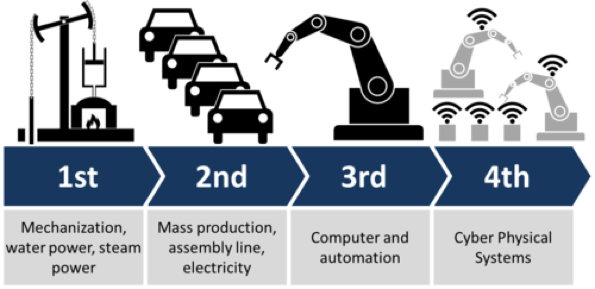
Since the concept was first articulated in 2011 by a German government-supported program promoting deeper integration of manufacturing software and hardware across the production value chain, the term “Industry 4.0” has gained recognition and momentum as the rallying cry for the 4th industrial revolution (see left Image by Christoph Roser at AllAboutLean.com). Wikipedia  summarizes it like this: “Industry 4.0 facilitates the vision and execution of a ‘Smart Factory.’ Within the modular structured Smart Factories of Industry 4.0, cyber-physical systems monitor physical processes, create a virtual copy of the physical world, and make decentralized decisions. Over the Internet of Things, cyber-physical systems communicate and cooperate with each other and with humans in real-time…” 

This definition may lead you to ask “What aspects of Industry 4.0 are truly revolutionary, and what technologies and tools are available today that would enable me to start building “Smart[er] Factories?” In this blog, I offer some potential answers to these questions that put the vision of Industry 4.0 within reach for automation practitioners familiar with the latest generation of SEMI Standards.  
IoT2.png

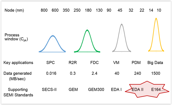
Semiconductor manufacturers have been collecting and using data from the equipment in their factories for decades. Throughout this period, device sizes and process windows have shrunk continuously according to Moore’s Law, and the SEMI Standards have evolved by necessity to support the insatiable demand for data exhibited by the process analysis and control applications that keep a modern fab running profitably (see left). The newest of these standards, the Equipment Data Acquisition suite (EDA, also known as “Interface A”), provides the power and flexibility to support a wide range of critical manufacturing applications and human users with ever-changing requirements; moreover, these standards can be deployed in a variety of system architectures without disturbing the “command and control” capabilities of existing factory systems.

“What does all this have to do with Industry 4.0?” To understand this, let’s look at the foundation of a “Smart Factory,” the collection of the many thousands of devices that might need to communicate over the so-called “Internet of Things.” 

We already see evidence that the availability of low-cost, low-power, networkable computing hardware will likely result in an explosion of “smart sensors” and other intelligent devices on the factory floor. However, as social scientists have observed over the millennia, groups of smart individuals don’t necessarily exhibit smart behavior in the aggregate, so what additional attributes must these devices possess to be good citizens of a collaborative, Industry 4.0 environment? How will these devices communicate effectively with one another? And what oversight will be required to ensure this communication achieves the ultimate manufacturing objectives?

As a starting point, I propose that each device, or manufacturing “thing,” at a minimum should be discoverable, autonomous, model-based, self-aware, communicative, and well-behaved. Depending on the role the device must play, it might also be self-monitoring, capable of defending itself (secure), and a consumer of data from other devices/systems as well as a provider. So defined, these devices would need a minimum of external monitoring and supervision (read “management overhead”) to perform their basic functions, but would rely on higher-level systems to provide specific objectives, instructions, and constraints (read “configuration, recipes, and limits”) for their operation in a given context and timeframe.

I realize that’s a lot to absorb at once, but now imagine that each of these devices could implement a subset of the services called for in the EDA standards, especially those defined in E120/E125/E164 (equipment modeling and standard metadata modeling), E132 (session management), and E134 (data collection management). Consider the collaboration among independent devices and systems this would enable…and ask yourself, how much closer to the vision of Industry 4.0 can you possibly get?

I hope the ideas above were useful…or at least thought-provoking. We’ll be developing this theme further in the coming months, but I wanted to use this blog as a conversation starter. We’d love to hear your feedback, so give us a call, or feel free to reach out to us.

Topics: Industry Highlights, Semiconductor Industry, EDA/Interface A, Smart Manufacturing/Industry 4.0