Industry News, Trends and Technology, and Standards Updates

Alan Weber: Vice President, New Product Innovations

Alan Weber is currently the Vice President, New Product Innovations for Cimetrix Incorporated. Previously he served on the Board of Directors for eight years before joining the company as a full-time employee in 2011. Alan has been a part of the semiconductor and manufacturing automation industries for over 40 years. He holds bachelor’s and master’s degrees in Electrical Engineering from Rice University.
Find me on:

Recent Posts

SEMI’s Smart Manufacturing Standards Survey: Usage, Requirements, Expectations, and Issues

Posted by Alan Weber: Vice President, New Product Innovations on Dec 7, 2022 10:30:00 AM

Earlier this quarter (October 2022) the SEMI Smart Manufacturing Council conducted one of its regular meetings with factory stakeholders to determine what sort of SEMI-sponsored activities could accelerate this important industry initiative. One focus area of the discussion was getting more and better data out of the sub-fab, since the performance and integration of these components is becoming more important for many of the leading manufacturers. The related, familiar topic of achieving better visibility into equipment and process behavior was also raised.

In that context, as it often does, the role of industry standards came up as a key enabling technology. The following question was posed: “Are the current standards sufficient to support the broad range of smart manufacturing use cases that factories envision, or does more need to be done? Specifically, since the Information and Control Committee is working on the Freeze 3 version of the EDA (Equipment Data Acquisition, also known as Interface A) suite of standards, are there problems that need to be addressed to improve the adoption of usage of these standards?”

This question triggered a lively (but non-convergent!) conversation among the participants in the meeting, many of whom have years (no, decades) of experience working in the standards community. Before long, it became clear that the group had no clear answer to these questions, and that more information from the actual user community was needed. Someone suggested that the Council pose the questions to a broader audience in survey form, and this proposal was enthusiastically accepted. Several of us volunteered to generate a draft survey for SEMI’s review and refinement, which got the activity off to a running start.

Given this opportunity to connect directly with the ultimate beneficiaries of SEMI Standards, there was a temptation to broaden the survey’s scope to cover other topics of interest in the smart manufacturing domain. Cognizant of the fact that the longer surveys have a lower chance of being returned with useful data, however, the group largely resisted this temptation, including the most important questions in an easy-to-answer format, leaving room for optional additional information in the responses for those so inclined.  

The final survey was issued by SEMI around October 21,2022 with a requested response date of November 15 (which has been extended to gather more feedback). Rather than repeat the entire content here, I include the following excerpts from the introduction and the table of contents:

The purpose of this questionnaire is to assess the status of the industry’s experience with and impressions of the SEMI EDA (Equipment Data Acquisition) standards suite to guide current and future initiatives that improve its capabilities, communicate implementation best practices, and foster broader adoption to realize the vision of SEMI’s Smart Manufacturing Community.

Respondents to this questionnaire should include companies that have already deployed the EDA standards in volume production as well as those that have yet to do so. Respondents in the latter category can simply skip the questions about current usage/issues.

The target audience was originally thought to be stakeholders in 300mm wafer fabs, but with the growing interest in enhanced data collection and automation for backend (packaging, assembly, and test) factories AND growth in the 200mm wafer fab segment (including new models of 200mm manufacturing equipment), it has been broadened to include these domains as well.  

Most questions are posed in multiple choice format, but additional detail is always welcome in the Comments fields where appropriate.

SEMI will compile the responses and share the result with the industry while preserving the anonymity of individual responses.

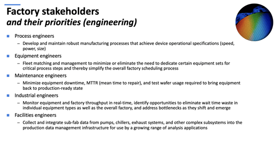
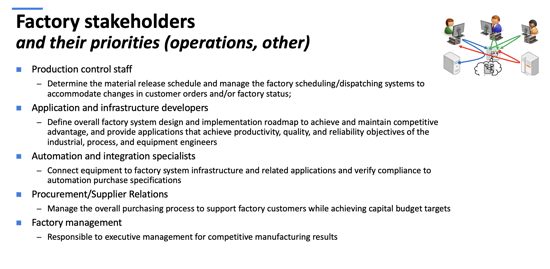
  1. Manufacturing Stakeholders
  2. Manufacturing KPIs (Operational Performance)
  3. Manufacturing Application Support
  4. Automation Requirements and Equipment Acceptance
  5. Current (or intended) Usage
  6. Issues and Expectations
  7. Other Data Collection Needs

Appendix – Stakeholders and Acronyms


Survey-SEMI-Blog-pic1A

Survey-SEMI-blog-pic2


Moreover, at this writing, the link to the on-line survey is still active here: 
à SEMI Equipment Data Acquisition / Interface A Standards Survey – Questionnaire on Usage, Requirements, Expectations, and Issues.

Finally, if you are interested in the details of the survey, and especially if you would like to provide your inputs directly to SEMI, you should contact Mark da Silva, Chair, SEMI Smart Manufacturing, Global Executive Committee, at mdasilva@semi.org.

And as always, to discuss your company’s specific Smart Manufacturing journey and to understand how we at Cimetrix by PDF Solutions can help, click on the contact button below. We look forward to hearing from you!

Contact Us


Topics: Industry Highlights, SECS/GEM, Semiconductor Industry, Doing Business with Cimetrix, Smart Manufacturing/Industry 4.0

Productivity Infrastructure for Smart Manufacturing

Posted by Alan Weber: Vice President, New Product Innovations on Feb 16, 2022 11:00:00 AM

With semiconductor factories worldwide running a full capacity in most market segments, it is no wonder that productivity is now an important careabout across the industry. Factory managers carefully monitor their Key Performance Indices (KPIs) for any indications of lost productivity so they can react quickly to identify and address the root causes of these excursions. At the same time, they question whether their productivity metrics are presenting an accurate picture of factory performance, since these tracking systems may have been in place for many years and not updated to leverage the full suite of available productivity standards and the associated data collection infrastructure.

If you are one of the people harboring such questions, this blog posting and the information conveyed in the underlying presentation are for you. In them, we highlight the key principles of productivity management in a complex manufacturing environment, describe the spectrum of SEMI standards that have been defined and refined over many years to support this process, identify the various data sources, collection methods, and system components necessary to implement them, and provide several concrete examples of how these pieces fit together.

Productivity Principles

Manufacturing productivity management can be tricky because there are inherent tradeoffs in some of the metrics (see intuitive illustration). Consequently, they must be considered as a set rather than individually…

  • Quality
  • Capacity
  • Throughput
  • Cycle time
  • WIP levels
  • On-time delivery
  • Equipment utilization

One of the most obvious examples is the conflict between equipment utilization and cycle time, especially in a wafer fab setting with reentrant, cyclical processes that use the same equipment multiple times. To minimize cycle time, you would want to ensure that product material never had to wait for equipment to become available. However, that will leave non-bottleneck equipment idle some of the time. On the other hand, if you maximize equipment utilization, WIP (Work in Process) levels will rise, degrading the cycle time for material queued for the next equipment type in its process flow. And so on.

SEMI Standards for Productivity Improvement

SEMI has a long history of defining standard metrics for the measurement and monitoring of equipment and factory productivity, but few, if any, companies take full advantage of these standards. Likely reasons for this include lack of awareness of what standards are available, limited understanding of what it takes to implement them, insufficient connectivity to the data sources required for a robust implementation, limited financial and personnel resources to build such a system, and no continuity of the subject matter expertise needed to oversee a comprehensive productivity management strategy. Daunting challenges, to be sure, but worthwhile to overcome in the current capacity-constrained environment.

This posting targets the first two of these challenges, and with the connectivity solutions in our product portfolio, we at the Cimetrix Connectivity Group of PDF Solutions can help address the third.

The SEMI standards that address Overall Equipment Effectiveness/Efficiency (OEE) include:

  • E10, E58 – Equipment Reliability, Availability, Maintainability (RAM, ARAMS)
  • E79, E116 – Measurement of Equipment Productivity, Equipment Performance Tracking

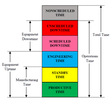
The principal objective of these standards is to account for every minute of an equipment’s life in the factory, dividing that time up into non-overlapping states to highlight and maximize the time spent in “productive” states while minimizing and identifying the root causes of the time spent in “non-productive” states. These standards have evolved over time from the initial definition of the six E10 equipment states (see figure below) to the definition of many useful sub-states, specification of formulas for calculating various measures of efficiency and “loss” categories based on these states, adaptation of these formulas to complex, multi-module equipment types, description of methods for automating the collection of event data that chronicle the transitions from state to state, and so on.

Productivity_infrastructure_image1It’s a lot of information to absorb, but each step along an implementation path can yield a return on that investment through the improvement of OEE-related KPIs.
A more recent but less familiar SEMI productivity standard has the same “account for every minute” objective but looks at the life cycle of the product material (lots, substrates, devices) in the factory rather than the equipment. These standards emerged from the Sematech “Wait Time Waste” initiative—now called Product Time Measurement—and consist of the following:

  • E168 – Specification of Product Time Measurement (terminology, concepts, time elements, etc.)
  • E168.1, .2, .3 – PTM for 300mm production equipment, Material Control Systems (MCS), and transport equipment (AMHS)

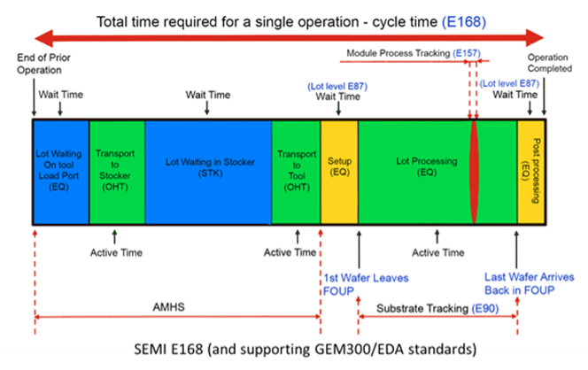
These standards divide product material time into two major states—“active” and “wait”—and then define explicit “time elements” (and associated GEM/GEM 300 begin/end triggering events) within those categories that describe what was happening to the material (processing, movement, outgassing, etc.) during its “active” time, and what/who it was waiting for (FOUP unload, robot arm, gate valve opening, recipe start, etc.) during its “wait” time. The figure below shows a sequence of wait and active time elements for a lot between the completion events of two contiguous process steps.

Productivity_infrastructure_image2Conservative estimates from factory operations managers familiar with the behavior of complex multi-chamber equipment suggest that there is 5-7% of untapped capacity in this kind of equipment that a product material-focused standard like E168 could expose and capture.
Infrastructure Implementation Technologies

After determining which of these standards you want to implement and to what extent, the remaining tasks deal with identifying the specific data sources/elements in the factory that must be connected to your data collection infrastructure and creating the pathways for this data to flow. Fortunately, over 95% of the information needed is referenced in at least one of the following SEMI standards suites:

GEM/GEM300

  • E30, E40, E94 – Machine States, Process Job Management, Control Job Management
  • E87, E90 – Carrier Management, Substrate Tracking
  • E157 – Module Process Tracking, Recipe Execution Tracking

Equipment Data Acquisition (EDA / Interface A)

  • E120, E125, E164 – Equipment Metadata Model
  • E132 – Authentication and Authorization
  • E134 – Data Collection Management

Moreover, there is plenty of commercial software available that implements these standards, so there is absolutely no reason to tackle this in-house. Nevertheless, the remaining challenge in this process is validating that the suppliers have faithfully implemented the standards in their equipment and that the semantics of the events called for in the productivity standards are consistent across the factory. For example, 300mm process equipment that provide a SEMI E164-compliant (EDA Common Metadata) EDA implementation will include the complete set of GEM 300 events with identical sets of state/event/parameter names. Other equipment interface implementations may have slight variations that require a custom mapping layer in the event handling.

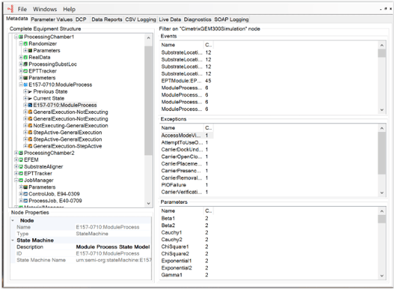
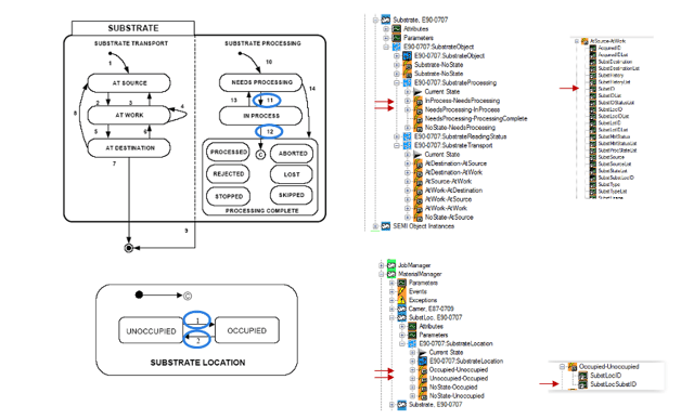
The figure below shows the E90 (Substrate Tracking) state machines used in some of the E168 time element definitions, and the corresponding E164-compliant metadata model content used to define the EDA Data Collection Plans (DCPs) that provide this information in real-time.

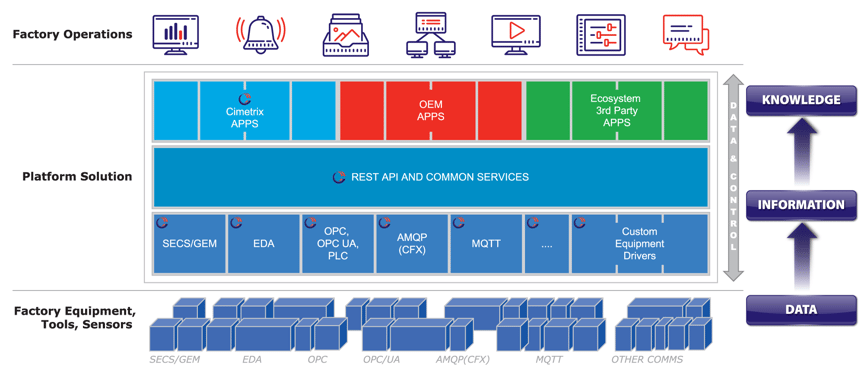
Productivity_infrastructure_image3On the “factory side of the wire,” it makes sense to incorporate modern commercial system technology as well, especially since a new productivity infrastructure could be implemented as a separate, complementary system rather than trying to squeeze it into an existing factory system architecture. A high-level diagram of a cloud-native instance of such a system is shown below. Note that it features a broad range of data source types (equipment, subsystems, sensors) using multiple connectivity standards (GEM, EDA, OPC UA, MQTT) at its lowest layer, all abstracted by a layer of RESTful APIs that in turn support a multi-supplier application ecosystem.
CMTX_PS_Sapience_Diagram_v5

Want to know more?

This material has recently been accepted for presentation at the 20th European Advanced Process Control and Manufacturing Conference (apc|m) in Toulon, France (4-6 April 2022) – we hope to see (or hear) you there. Between now and then, you can access a preview copy here, and feel free to contact us with any questions.

Contact Us

Topics: Industry Highlights, Semiconductor Industry, Doing Business with Cimetrix

Backend Automation Highlighted in Smart Manufacturing Pavilion at SEMICON West

Posted by Alan Weber: Vice President, New Product Innovations on Jan 5, 2022 11:15:00 AM

SEMICON West 2021 wrapped up last month and despite being a hybrid event with limited attendance, there was nevertheless a lot of excellent technical information available through the various SEMI-organized programs. One such program was the Smart Manufacturing Pavilion which featured a series of “Meet the Experts” presentations on Tuesday afternoon, December 7.

Our own Alan Weber (VP of New Product Innovations) was privileged to be included, and his talk was titled “Accelerating Advanced Backend Automation through Smart Application of Frontend GEM 300 Standards.” The presentation was co-authored by Michael Kollex, Swee Shian Yap, and Olaf Herzog of Infineon Technologies, who also developed and contributed much of the technology that was discussed. But we’re getting ahead of ourselves…

Background

Automating assembly, packaging and test facilities has always faced challenges not seen by their upstream wafer fab counterparts. These include (but are not limited to):

  • Multiple material transformations (and associated carrier types)
  • Linear flow shop manufacturing operations (vs. cyclical)
  • High product variety and velocity
  • Significant manual intervention
  • Complex unit product traceability requirements
  • Low (relative to wafer fab) equipment cost and automation budget
  • Equipment supplier un-familiarity with SEMI Standards
  • Handling multiple data source types/protocols

In mid-2019, a new SEMI Standards task force—the Advanced Backend Factory Integration Task Force (ABFI TF)—was created to address these challenges.

An important operating principle of this task force is to ensure that any new standards identified for the assembly and packaging segments are not only technically consistent with the existing body of connectivity and control standards but also directly leverage as much of the current SEMI automation standards as possible. This is especially important for the capabilities covered by the GEM 300 (Generic Equipment Model) standards since GEM is already well adopted by many of the equipment suppliers to the backend assembly, packaging, and test market.

However, this still leaves a gap that must be filled by the automation requirements for each factory customer, which is precisely what the work described in this presentation accomplishes in a way that serves the entire industry.

Solution Approach

The approach to this problem features several key innovations.

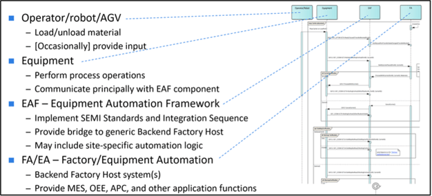
The first key innovation is the definition of a detailed “Target Equipment Integration Sequence” applicable to all equipment types that supports full automation of assembly and packaging operations while eliminating the ambiguity that raises implementation costs for equipment suppliers and factory engineers alike. The scope of this sequence for a given unit of equipment covers its entire operation, from loading material carriers and verifying their content; mounting, usage tracking, and unmounting of consumables and durables that are directly associated with the products being manufactured (a key traceability requirement); creating the process/control jobs appropriate for that material and retrieving the associated process recipes; tracking execution of those jobs and accumulating the data items required for single device traceability; storing that data in the substrate map data structures; and passing that information back to the factory systems.

The specific expression of this integration sequence is a ladder diagram of the system communication partners, which include an operator/robot, the equipment, an Equipment Automation Framework (data collection server), and the Factory Information and Control System(s). This is shown in the figure below.

Backend-pic1The second key innovation is basing the messages that constitute this sequence on existing, mature SEMI GEM 300 standards, thereby reducing (and eventually eliminating) the need for custom implementation software. Amazingly, except for the need to support “nested carriers,” realizing the integration sequence requires almost no modifications to the existing GEM 300 standards.

The third key innovation is realizing this integration sequence in a sample application suite to bring the specification to life and provide a reference implementation to accelerate the development process. This includes 1) an equipment simulator that faithfully implements all the capabilities called for in the integration sequence, 2) a sample factory host application that serves as the principal communications partner for the equipment during the implementation of the integration sequence by a specific equipment supplier, and finally 3) a set of automated tester “plug-in” modules for validating that the equipment-side implementation has in fact met the requirements. Together these software modules greatly reduce the time it takes to understand, implement, and test these important new specifications. This software suite is depicted in the figure below.

Backend-Pic2The fourth innovation is more procedural than technical: by openly sharing this design with the industry standards community, we believe it will be enhanced and further generalized by other assembly and packaging thought leaders, increasing the level and sophistication of overall automation capability while lowering integration and operation costs across the industry.

What’s Next?

Next steps include promoting this design to potential stakeholders through webinars and regional training events, gathering and incorporating feedback into the key artifacts, and validating its applicability in multiple manufacturing sites.

Where Can I Get the Presentation?

A fully narrated version of the presentation is available here; we hope you find it useful, and please contact us with any questions. We wish you the very best on your company’s backend automation – let us know how we can help!

Ask an Expert

Topics: Industry Highlights, Semiconductor Industry, Doing Business with Cimetrix

All You Could Ever Want to Know about Smart Manufacturing – in a Two-Volume Treatise

Posted by Alan Weber: Vice President, New Product Innovations on Aug 26, 2021 1:15:00 PM

A little over 3 years ago, the Elsevier publishing company decided that the topic of Smart Manufacturing had achieved enough global breadth and momentum to warrant in-depth treatment in an edited set of articles. As they researched the domain, they realized that it split neatly into two categories of material: a general set of concepts that are applicable in any industry, and example implementations that are specific to a small set of related industries.

The editors then consulted with a number of industrial and academic subject matter experts to subdivide each category into a set of topics, and the Table of Contents for each of the two volumes was born. The results were first published in August 2020, and are available from Elsevier:

  • Volume 1: Concepts and Methods (426 pages) 

    “Research efforts in the past ten years have led to considerable advances in the concepts and methods of smart manufacturing. Smart Manufacturing: Concepts and Methods puts these advances in perspective, showing how process industries can benefit from these new techniques. The book consolidates results developed by leading academic and industrial groups in the area, providing a systematic, comprehensive coverage of conceptual and methodological advances made to date.”

  • Volume 2: Applications and Case Studies (528 pages) 

    “Research efforts in the past decade have led to considerable advances in the concepts and methods of smart manufacturing. Smart Manufacturing: Applications and Case Studies includes information about the key applications of these new methods, as well as practitioners’ accounts of real-life applications and case studies.”

One of the editors was Dr. Thomas F. Edgar, a long-time professor in the University of Texas Chemical Engineering department who specialized in process modeling, control, and optimization. He is also credited by many as being the “father of semiconductor APC" (advanced process control), since a number of his graduates ended up in the automation/process engineering department at AMD/Austin and transformed this domain from spreadsheets and “sneakernet” to a fab-wide, model-based process control system.

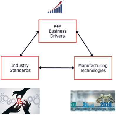
Needless to say, I was honored when he called to say that Elsevier wanted a case study on the semiconductor industry’s use of smart manufacturing, and to ask if I would write that section. I readily agreed, and provided the chapter titled “Smart Manufacturing in the Semiconductor Industry: An Evolving Nexus of Business Drivers, Technologies, and Standards.” The abstract for that chapter follows:

“The semiconductor industry embarked on its own “Smart Manufacturing” journey well over 30 years ago, long before the term was coined. The continuous productivity improvements that we now take for granted are essential for creating and building the devices that fuel our electronics-based global economy and maintaining commercial viability in a hypercompetitive industry. However, what we have learned in the process is that like many scientific endeavors, it is a journey without a destination. As new market opportunities are met with new device and system technologies in an ever-changing business environment, the list of manufacturing challenges is never complete.

This is where the global Smart Manufacturing initiative enters the picture. Although its key tenets are not specific to the semiconductor industry, the attention it drew to this topic triggered the formation of the SEMI Smart Manufacturing Community, which now provides a forum for thought leaders across the semiconductor manufacturing value chain to focus on these important challenges. To put this initiative in its proper perspective, this chapter explores the past, present, and future of Smart Manufacturing in the semiconductor industry.”

Regarding the Smart Manufacturing Initiative (now with chapters in several geographic regions), SEMI is the perfect host for such a group. Since its charter includes both trade and standardization activities for the industry worldwide, and its members develop the diverse technologies that comprise the electronics industry, SEMI forms an ideal backdrop for describing the evolution of semiconductor Smart Manufacturing. This is illustrated in the figure below.

Smart-manufacturing-two-volume-image

Thinking back over my almost 50 years in the industry, I think the factor that contributed the most to the industry’s current success was the evolution of its collaboration culture. Whether driven by the need for industry efficiency, the fear of extinction, or the recognition of mutual interdependence, today’s global semiconductor industry enjoys a collaborative culture that is unequaled in other for-profit industries.

If the topic of Smart Manufacturing piques your interest, I invite you to visit the Elsevier websites shown above for more information. I have also distilled the semiconductor case study chapter into a set of slides that I will be happy to review/discuss with you.

We wish you the best on your company’s Smart Manufacturing journey – let us know how we can help!

Ask an Expert

Topics: Industry Highlights, Smart Manufacturing/Industry 4.0, Machine Learning

Machine Learning in Smart Manufacturing: Technologies You Should Be Tracking Now

Posted by Alan Weber: Vice President, New Product Innovations on Jun 3, 2021 11:45:00 AM

shutterstock_510171997-1We’re drowning in data but still thirsting for wisdom… This is a paraphrase of what one of the virology doctors interviewed at the beginning of the COVID-19 pandemic said about the challenges they faced in charting a course of action using the myriad volumes of data being collected around the world. The sentiment reminded me that in an entirely separate but no less complex domain: electronics manufacturers face similar challenges using data from the thousands of disparate sources in a factory to make the decisions that ultimately determine the viability of their enterprises.
To the extent that these two domains have a similar problem statement, they also share a set of solution technologies. Among them is Machine Learning (ML), which is a promising subset of Artificial Intelligence (AI). The essence of Machine Learning is using data collected from past events to develop and train a model that can make reliable predictions about the outcome of future, as-yet-unseen events.

Machine Learning technology is already more ubiquitous than you might imagine. For instance, if you’ve ever 1) ordered one of Amazon’s product recommendations based on your previous purchases and search history, 2) seen the names on the faces of people in your photo library (and updated the ones it got wrong), 3) rated your satisfaction with a Netflix movie you’ve just watched, or 4) interacted with one of the language translation apps on your smart phone, congratulations—you are now an integral part of the Machine Learning ecosystem of the suppliers of those everyday products.

Beyond these familiar examples, two factors have contributed to the rapid ascendance of ML as a viable production technology: the availability of massive amounts of data and affordable storage and processing power to analyze it. As a result, Machine Learning is now seen as a key enabling technology for Smart Manufacturing in multiple industries and at multiple positions along the value chain.

Documented use cases in semiconductor front-end factories include production scheduling and dispatching, process analysis and excursion prediction, equipment FDC (fault detection and classification), preventive maintenance, failure prediction, trace data analysis, and so on. Equipment suppliers are likewise looking for ways to add value to their products by offering ML-based capabilities as an option. Semiconductor back-end and SMT factories and their respective equipment suppliers are also actively evaluating ML technologies. These instances all have one thing in common: the need for quality equipment data… and lots of it.

Two of the most prevalent approaches to Machine Learning are 1) supervised learning, which uses labelled data samples to develop a model that predicts the labels for future samples; and 2) unsupervised learning, which can use unlabeled data samples to develop a model of expected behavior that can predict deviations from that behavior for future samples.

Both categories have direct applications in manufacturing and include a range of specific algorithms that may be suited to various problem types. The trick is knowing which technique(s) to apply in which situations, and once chosen, how to tune a particular technique for a given problem.
machine-learning1.1

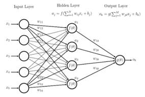
One category of public-domain algorithms that has shown significant promise for commercial applications has been labelled “Deep Learning,” and it refers to a variety of “Artificial Neural Net” approaches. These algorithms fall into the supervised learning category but can nevertheless be applied in situations where the labels are not known a priori (e.g., analyzing system log files to detect anomalous behavior).

A frequently-cited candidate for a supervised learning algorithm is predictive maintenance, which uses as input a high-dimensional (i.e., lots of parameters) trace vector of equipment parameters with a binary label (“good” or “failed”). With enough production history this data can be used to train and validate a failure prediction model that would improve on the “run to fail” or “just in case” maintenance strategies used today.

Likewise, a good candidate for unsupervised learning is anomaly detection using equipment log file data (could also include trace data) as input. Many equipment suppliers save this kind of data for “after the fact” analysis of problems that occur in manufacturing without a clear sense of what might be useful. Deep Learning algorithms are particularly adept at using high dimensional data to create complex mathematical models that represent “normal” behavior and can be used to flag “abnormal” behavior as it happens.

From an implementation standpoint, there is no “one size fits all” Machine Learning package or library that can address the full range of potential opportunities. Moreover, since Machine Learning is only a component (albeit a vital one) of an overall solution system, it is important to understand how all the pieces fit together when considering these technologies for a specific problem. Subsequent posts in this series will explore these topics in greater detail, so stay tuned for additional information about how to map these new technologies into your product and problem space. However, if your need is more urgent, click the button below to see how we can explore this exciting new area together.

Contact Us

Topics: Industry Highlights, Smart Manufacturing/Industry 4.0, Machine Learning

18th Innovation Forum for Automation: Successful Transition of an Important Tradition

Posted by Alan Weber: Vice President, New Product Innovations on Mar 17, 2021 1:45:00 PM

Dresden-christmas-marketNear the end of January for almost two decades, the companies that form the Automation Network Dresden (AND) have hosted a gathering of semiconductor automation professionals in the picturesque setting of Dresden, Germany. The chill of winter during this event has always been in stark contrast to the warmth of the reception the speakers and participants enjoy at this event. The big question this year was “how could the organizers possibly maintain this tradition amid the COVID-19 pandemic and its travel restrictions?"
Automation people being a creative bunch, they responded by offering a series of free, half-day “digital events” spread across the first four months of the year, and each hosted by one of the AND member companies: SYSTEMA, Fabmatics, XENON, and Kontron AIS. The first two sessions are now in the record books, and as a participant in both, I can attest that no momentum or value has been lost. The only exception is the lack of the forum’s famous evening event, which will undoubtedly return next year when the virus is behind us.

The first session of the year was hosted by SYSTEMA on January 28 with the theme of Datafication and Automation: The new normal for semiconductor manufacturing. I was privileged to among the invited speakers, and shared the agenda with Manfred Austen of SYSTEMA (always a hard act to follow!), Jean-Marc Philippe of ST/Micro Singapore, Axel Wogawa of SYSTEMA, and Klaus Kleilein of Fabmatics.

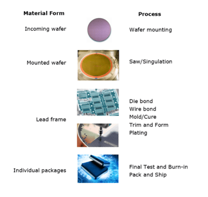
In this context, I chose the topic of semiconductor backend automation, and you can download my presentation “Wafer Fab Best Practices for Backend Automation”. Key takeaways from this presentation include the industry drivers for higher levels of backend automation, the unique challenges this poses when compared to wafer fab automation (see the figure highlighting multiple material transformations below), the role that industry standards in many categories will play in this process, and last but not least, the importance of defining explicit integration message sequences between all the equipment and the factory systems that bring them together into fully automated operations. This latter insight was one of the key enablers for the wafer fab transition from 200mm to 300mm, and the concept equally applies in the backend.

18-innovations-forum-pic1The second event in the series was hosted by Fabmatics on February 25, 2021, with the enticing theme of Forever Young: Automation Makeover Rejuvenates Golden Age Fabs. It featured speakers from Bosch, Nexperia, Cohu, and SYSTEMA.

The next event will be hosted by Xenon on March 25, 2021 with the theme Digitalization Meets Mechanical Engineering, and the final event hosted by Kontron AIS on April 29, 2021 (theme still TBD – stay tuned). For more information about this digital event series, visit the Automation Network Dresden website.

For help in crafting and executing your own backend automation strategy, or any other topic related to advanced manufacturing connectivity and control, please contact us by clicking the button below. 

Ask an Expert

Topics: Industry Highlights, Events, Smart Manufacturing/Industry 4.0

Thinking Ahead: Why would I want to buy EDA client libraries for my equipment?

Posted by Alan Weber: Vice President, New Product Innovations on Nov 11, 2020 11:30:00 AM

Background and Audience

Over the past several years, I have written numerous blog postings heralding the benefits of the SEMI Equipment Data Acquisition (EDA, also known as Interface A) standards, promoting their adoption by 300mm wafer fabs around the world, explaining how to develop robust purchase specs to ensure the interfaces delivered by the equipment suppliers meet the fab customers’ expectations, describing how the various components of the standards work together and the importance of the embedded equipment model, and finally explaining how to run compliance and performance tests on an EDA interface to validate its fitness for production use. The target audience for most of these postings has been the factory users, for they are the ones who increasingly depend on detailed equipment and process data to profitably run their enterprises.

By contrast, this posting is aimed at the equipment suppliers who are looking to increase the value of their product families by augmenting their hardware offerings with software capabilities that only they are uniquely qualified to provide.

This is not a new idea. Several major equipment suppliers have offered so-called “Equipment Engineering Systems (EES)” products as companions for their equipment over the years, providing applications like Fault Detection and Classification (FDC), production monitoring, maintenance management, local repositories for diagnostics and field support, and other capabilities that leveraged deep domain knowledge of the equipment. However, these systems necessarily relied on private interfaces to the equipment for their data, such as an additional network connection, direct access to the file system, or other mechanisms. And from the fab’s perspective, these constituted yet another piece of infrastructure to maintain.

Now there’s EDA: a key enabler for value-added equipment applications

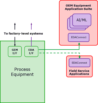
Since the SEMI EDA standards are inherently multi-client, a single EDA interface can support not only the factory information and control systems that depend on equipment data, it can also provide whatever information a supplier-specific application may need as long this data is represented in the equipment metadata model. Since that model is designed by the equipment suppliers as a fundamental component of the EDA interface, they can choose to put as much information in these model as they want, possibly well beyond that required by the fab customers’ purchase specifications. In fact, these models could be used to implement the diagnostic logging capability that suppliers usually build into their equipment for their own use, but without requiring custom software to read and interpret that information. See the figure below for an example of such a configuration.

EDA-Equipment-1The EDA standards also include a provision for “built-in DCPs” (DCP = Data Collection Plan) which can be shipped with the equipment and protected from accidental deletion at the factory site. These DCPs could be crafted by the equipment supplier to directly feed whatever value-added applications the supplier chose to develop, whether these resided on a computer local to the equipment in the fab, on portable computers used by field service engineers to diagnose problems, or on remote cloud-based systems allowed to connect via secure EDA-defined URLs. This flexibility opens up a wide range of application types, from those that embed equipment-specific algorithms to generic Machine Learning frameworks… the possibilities are endless.
What all these approaches have in common is a standard EDA client capability that can establish a session with the equipment, activate Data Collection Plans, and receive the ensuing Data Reports. The EDAConnecter within the Cimetrix Sapience platform provides all these features and more in a lightweight set of .NET libraries which can be deployed wherever they are needed to consume EDA data.

Conclusion

More and more semiconductor factories are requiring EDA interfaces with their new equipment purchases with highly prescribed equipment models and demanding performance criteria. From the equipment supplier’s perspective, these requirements have been viewed as a source of additional cost, with all the benefits accruing to the factory customers. But it doesn’t have to be that way…

Why not take advantage of this interface to offer additional value using a standards-based approach? This just might be an idea whose time has finally come. If you agree, give us a call – we can help you make it happen!

Topics: Industry Highlights, Semiconductor Industry, EDA/Interface A, Doing Business with Cimetrix, Standards

Semiconductor Backend Processes: Tracking Process Execution

Posted by Alan Weber: Vice President, New Product Innovations on Sep 30, 2020 11:45:00 AM

Background

semi-e157-pic1

Previous blog posting in this series have discussed the rationale for using SEMI’s GEM, GEM 300, and related automation standards in semiconductor backend factories, and pointed out that the specific adaptations required for the various backend equipment types are one of the focus areas for the SEMI Advanced Backend Factory Integration (ABFI) Task Force. In this posting, I will deal specifically with the benefits that can be realized by using the E157 Process Module Tracking standard in a backend factory context.

Since none of the backend material transformations are implemented in what front end experts would consider a “process chamber,” this may seem like an unlikely fit. Moreover, the velocity of backend processes seems contrary with the typical front end recipe execution paradigm. Finally, the lack of distinct substrate locations for some of the processes makes it difficult to know precisely when the process begins and ends for the affected material in some cases.

Regardless of these challenges, the requirements for single device traceability that include knowing the exact process conditions that a device was exposed to at every moment in its manufacturing life cycle (including the backend) argue for use of this standard wherever possible.Since none of the backend material transformations are implemented in what front end experts would consider a “process chamber,” this may seem like an unlikely fit. Moreover, the velocity of backend processes seems contrary with the typical front end recipe execution paradigm. Finally, the lack of distinct substrate locations for some of the processes makes it difficult to know precisely when the process begins and ends for the affected material.

SEMI E157 – Process Module Tracking

The purpose of SEMI E157 is “to define a standard equipment capability to report process-related data to the factory system… the activities of a processing location (i.e., process module) that are related to the execution of a recipe.” The standard further states that “the collection of process data during recipe execution is important to today’s semiconductor factories to support various applications that help optimize equipment processes, finished product quality, yield, and overall factory performance.”

These requirements are now every bit as important for backend factories as they are for the front end, so it is useful to understand how E157 can be effectively applied.

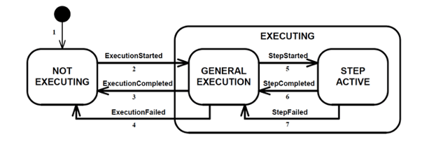
First of all, the E157 Module Process State Model is fairly simple, having only 4 states (three of which are “base states” with no sub-states) and 7 state transition events, shown in the diagram below.

E157-pic1This model represents the state of that portion (or portions) of a unit of equipment that executes a recipe to transform whatever material is present in that part of the equipment. In front end equipment, the chambers are relatively distinct, and usually process a small number of substrates (often one) at a time. By contrast, backend processes cover a broad spectrum of material types, from single wafers to strips (or lead frames) of multiple die to individual packages. The material flow characteristics also vary, from discrete (i.e., single workpieces) to batch to continuous. Moreover, the production rates and material volumes for these processes range from perhaps 90 wafers per hour to thousands of packages per hour… With these challenges, it is no wonder that the pace of automation for these facilities has lagged that of the front end.

How is the E157 Standard Used?

From the equipment’s perspective, every time the process module changes state according to the model above, the equipment sends the corresponding state transition event to the factory host computer. This is done using the SECS-II S6, F11 Event Report message with an event name exactly prescribed by the E157 standard.

The event report should also include whatever “context information” from the equipment that the factory applications need to analyze the equipment’s performance and behavior. For some backend processes, this might be lot ID, process job ID, recipe name, control settings, and current parameter values for important process variables. For others, it might be cumulative usage counts for fixtures with limited lifetimes, current levels of consumables used in the process, or configuration parameters for equipment with a range of setup possibilities. To further complicate matters, some of this information is common across most processes, some of it is process-specific, but some of it may actually be vendor-specific. It all depends on how the factory operates.

Finally, when used in conjunction with event timing information from other required standards (e.g., E90 Substrate Management), E157 data can help identify potential productivity issues, say, when there is an unexpected delay between material arrival (from E90) and recipe start (E157).

How Might E157 be Adapted for Backend Equipment?

As noted above, some equipment types process a stream of material continuously. In these situations, for a given lot, multiple substrates may be processed at the same time in a continuous flow (say, on a conveyor through an oven) until the lot is complete. For these types of equipment, E157 cannot be directly applied because it is chamber oriented, and you don’t get much useful information if you use the entire lot as the execution starting and completing events.

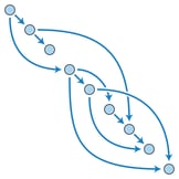
However, if you apply the same state model to the material (substrate, strip/lead frame, carrier, etc.) being processed rather than the equipment component, the collection events defined by E157 can be implemented when a unit of that material changes state. Specifically, the equipment can report the same collection events (ExecutionStarted, StepStarted, StepCompleted, ExecutionCompleted, StepFailed and ExecutionFailed) when execution on a substrate changes state, including when a step is started and completed. The meaning of a “step” would still be interpreted and designed by the equipment supplier. Associating these E157 collection events with a new “substrateID” data variable rather than a chamber enables the factory user to track the material state for each substrate going through the equipment.

Which Backend Equipment Types Should Implement E157?

Even though backend metrology, inspection, and test equipment may run recipes to perform their tasks, since no material transformation takes place, the state transition events and related context are far less important than the measurement and inspection results that these equipment types generate.
For the rest of the backend processes, the relative priorities for implementing E157 are the following:

High – die attach, wire bonding, dicing/sawing/singulation

Medium – backside grinding, polishing, plating, annealing molding, trim and form

Low – wafer mounting, die glue curing, deflashing, laser marking, tie bar cut, baking, burn-in

One category of equipment we have not mentioned is custom assembly equipment that can vary greatly by the end product form factor. The use of E157 in this equipment will depend entirely on the process complexity and sources of variability that must be tracked. However, it is safe to assume that for all but the simplest of processes, E157 will likely play a useful role.

Conclusion

E157 is a prime example of an exceptionally simple and well-written standard built on top of GEM technology that is easy to implement and provides a lot of end user value. The SEMI ABFI task force is now evaluating the specific adaptation of E157 for various backend equipment types and welcomes your contribution to that process.

Topics: Industry Highlights, Semiconductor Industry, Smart Manufacturing/Industry 4.0, GEM300

Are you now required to work from home? Don’t let it cripple your EDA-related activities!

Posted by Alan Weber: Vice President, New Product Innovations on Mar 25, 2020 1:15:00 PM

WFHEDA1The COVID-19 pandemic is impacting businesses worldwide, and in many regions, working from home is now mandatory or at least strongly encouraged.
While this doesn’t pose a major disruption for many types of jobs, it can be problematic for people working with the automation features of advanced manufacturing equipment. The network connections to production equipment are normally part of a secure factory system infrastructure, which makes them almost impossible to reach from outside the company’s intranet. Luckily, for those responsible for testing and characterizing the SEMI EDA (Equipment Data Acquisition, also known as Interface A) interfaces on new 300mm equipment, this should only be a minor inconvenience. And why is that?

The choice of internet technologies (Web Services, SOAP/XML) as the foundation for the EDA standards makes it easy to connect to a piece of equipment over the internet as long as the user’s client computer can “reach” the connection URLs of the equipment (and vice versa). What this probably means in practice is setting up a VPN (Virtual Private Network) connection from your client computer (say, the laptop you normally use) to the company’s network. This is something that road warriors and remote employees must often do as a matter of course to access internal file systems, in-house applications, and other private information.

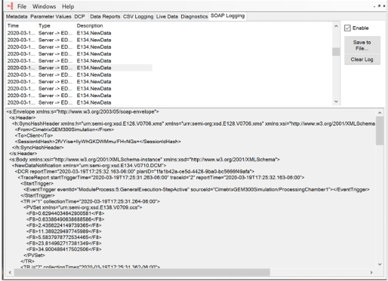
Once this is done, you can connect to the various service URLs for that equipment by including the remote computer name in the session connection strings. Note that you may have to modify the firewall settings of your client machine so the E134 NewData messages can find their way back to you. This is necessary because these are NOT request/reply messages like many of the EDA services; rather, they are initiated from the equipment, so your application has to be listening for them on the Consumer URL. This address is passed to the equipment when the connection session is first defined and established.

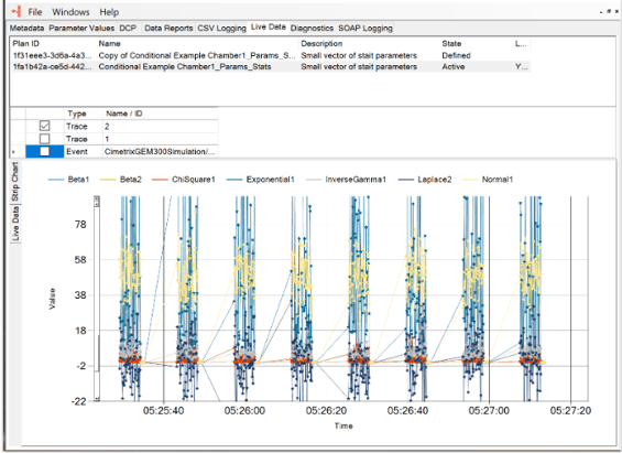
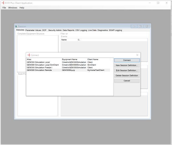
Using the Cimetrix ECCE Plus client product as an example, here is how I would set up a remote (from home!) session with an EDA-enabled 300mm equipment simulator running in our office on a machine named “edasimulator.” The first screenshot shows the choice of connections defined for my instance of the ECCE Plus; note that last one in the list that is highlighted.WFHEDA2png

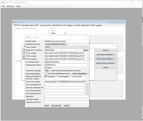
Clicking on the “Edit Session Definition” button and then the “More >” checkbox yields the screen below. You can see that the equipment IP address is “edasimulator” (the remote computer name referenced above) and each of the Freeze II service URLs (E132 Location, E125 Location, and E134 Location) for the session are defined on that machine.WFHEDA3

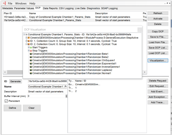
Note that the client ID (From/Client Name), which is “MyHomeTestClient,” must also be defined in the equipment’s Access Control List (ACL). For me to be effective, this client must have sufficient privileges for the kinds of work I need to do, which may include using existing DCPs (Data Collection Plans), creating additional DCPs, viewing interface configuration parameters (e.g., Max Sessions) and ACL entries, browsing the metadata model, and looking at the SOAP logs. Results of some of these tasks using the ECCE Plus are shown below.WFHEDA4WFHEDA5pngWFHEDA6WFHEDA7png

This may sound like a lot of trouble, but with a little help from your company’s IT support team, you can follow the “shelter in place” guidelines and STILL work effectively on your EDA-related tasks. And when the current crisis has passed, you’ll know how to be even more effective when you’re on the road!

We hope the posting is useful for you, and most importantly, that you and your loved ones stay safe and calm.

Topics: Industry Highlights, EDA/Interface A, Customer Support, Partners, Doing Business with Cimetrix

Advanced Process Control Conference XXXI:  Retrospective and New Standards News

Posted by Alan Weber: Vice President, New Product Innovations on Nov 11, 2019 9:15:00 AM

APC2019-1The 31st annual APC Conference is now in the history books, and the diversity of topics, presenters, and local distractions made it well worth the visit to San Antonio! This year’s agenda featured half-day tutorials on the basics of APC and cyber-security, keynotes from chip makers and leading suppliers on automotive industry requirements, smart equipment, and smart manufacturing, and a series of packed technical sessions covering sensors and equipment control, fault detection and feedforward/feedback control, advanced analytics, and standards.
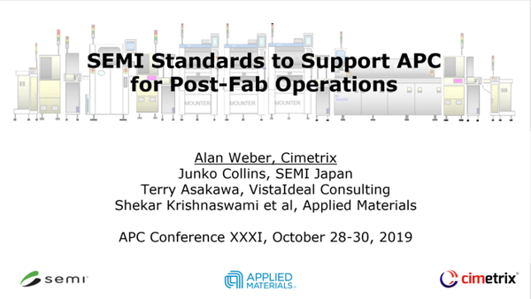
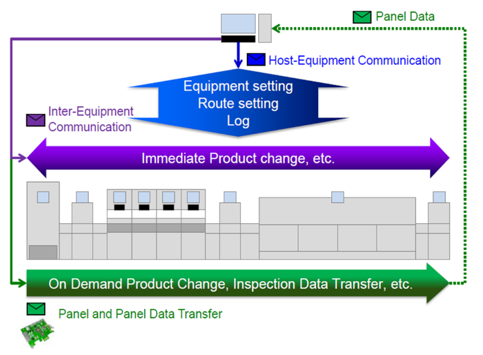
One of the presentations in the standards session provided detailed information about the new SEMI SMT-ELS (Surface Mount Technology Equipment Link Standards) M2M (machine-to-machine) communications standard. Alan Weber made the presentation titled “SEMI Standards to Support APC for Post-Fab Operations” to an interested audience, which triggered a number of discussions about the automation roadmap for the semiconductor assembly and test segment. This was especially relevant, since some of the leaders of the newly formed SEMI Advanced Backend Factory Integration Task Force (ABFI TF) were also present.

APC2019pic2The SMT-ELS standard has come a long way in a short time, and the ambitious, integrated demonstration created by 4 major SMT suppliers (Fuji, Juki, Panasonic, Yamaha) that was exhibited in June (Japan) and August (China) will again be shown in productronica (Munich, 13-15 November). The basic functions of SMT-ELS (officially designated at SEMI A1, A1.1, and A2) appear in the figure below.
APC2019pic3Cimetrix will likewise demonstrate this new standard at productronica, showing not only an equipment-level implementation of the M2M features but also the host-based configuration process and a plug-in for doing protocol validation tests.
Smart Manufacturing was a common theme this year, with an entire session dedicated to this global initiative. The Factory Integration section of the IRDS (International Roadmap for Devices and Systems) will be reorganized around the tenets of Smart Manufacturing, and a two-volume multi-industry book on this body of technology is scheduled for publication early next year. Another of Alan Weber’s presentations was dedicated to this topic, as he wrote the chapter chronicling the semiconductor industry’s development and use of these technologies.

APC2019pic4If you would like any further information, you can speak with a Cimetrix expert, or you can stop by our booth at productronica this week (Hall A3 booth 451). 

Ask an Expert

Topics: Industry Highlights, Doing Business with Cimetrix, Events, Smart Manufacturing/Industry 4.0