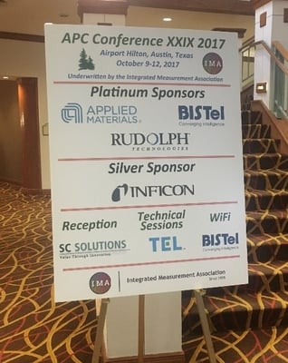
 Austin, Texas was the site of this year’s conference, going back to its roots after almost 30 years. Because of its unique focus on equipment and process control technology for the semiconductor industry, and the consistently high quality of its technical content, this conference continues to attract both industry veterans and newcomers to this domain, with this year’s attendance over 160.


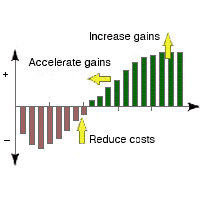
Cimetrix has been a regular participant and presenter at this event, and this year was no exception. Alan Weber made a presentation entitled “ROI-based Approach for Evaluating Application Data Collection Use Case Alternatives” that was jointly developed with Mark Reath of GLOBALFOUNDRIES. The key message of this talk was that data collection should not be viewed as an all-or-nothing proposition but rather a spectrum of alternatives within which an approach can be chosen that best fits the problem to be addressed. As examples, the presentation described specific FDC use cases that resulted in significant savings through reduced false alarm rate and fewer/less severe process excursions. For a copy of this presentation, follow the link at the bottom of this posting.
 Boyd Finlay’s (GLOBALFOUNDRIES) keynote presentation was undoubtedly one of the highlights of the conference. His presentation, “Raising the Bar: Foundry Expectations for Equipment Capability and Control,” painted a compelling picture of how future semiconductor manufacturing equipment must be able to support the growing demand for semiconductors in almost all aspects of modern life, especially in self-driving cars and their supporting infrastructure. For example, one of the specific expectations is that “Fab engineers expect fully integrated instrumentation on and around equipment to provide well established unambiguous high-volume manufacturing sensor supporting BKMs (best-known methods).” This presentation is well worth your time to review regardless of your job function in the industry, so follow the link below for a copy.
Samsung also offered some very interesting insights in a presentation titled “Wafer Level Time Control for Defect Reduction in Semiconductor Manufacture FABs.” It correlated defect densities to position in the FOUP and explained 2 sources for these: 1) outgassing of wafers after certain kinds of processes (which can be addressed with N2 purging), and 2) the difference in post-process waiting time, which must now be considered at the individual wafer level rather than the lot as a whole.
This conference and its sister conference in Europe are excellent venues to understand what manufacturers do with all the data they collect, so if this topic piques your interest, be sure to put these events on your calendar in the future. In the meantime, if you have questions about any of the above, or want to know how equipment connectivity and control fit into the overall Smart Manufacturing landscape, please contact us!


